FDS4470 Datasheet and Replacement
Type Designator: FDS4470
Type of Transistor: MOSFET
Type of Control Channel: N
-Channel
Pd ⓘ
- Maximum Power Dissipation: 2.5
W
|Vds|ⓘ - Maximum Drain-Source Voltage: 40
V
|Vgs|ⓘ - Maximum Gate-Source Voltage: 20
V
|Id| ⓘ - Maximum Drain Current: 12.5
A
Tj ⓘ - Maximum Junction Temperature: 175
°C
tr ⓘ - Rise Time: 12
nS
Cossⓘ -
Output Capacitance: 605
pF
Rds ⓘ - Maximum Drain-Source On-State Resistance: 0.009
Ohm
Package:
SO-8
-
MOSFET ⓘ Cross-Reference Search
FDS4470 Datasheet (PDF)
..1. Size:146K fairchild semi
fds4470.pdf 
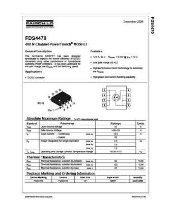
December 2006 FDS4470 40V N-Channel PowerTrench MOSFET General Description Features This N-Channel MOSFET has been designed 12.5 A, 40 V. RDS(ON) = 9 m @ VGS = 10 V specifically to improve the overall efficiency of DC/DC converters using either synchronous or conventional Low gate charge (45 nC) switching PWM controllers. It has been optimized for low gate charge
..2. Size:258K onsemi
fds4470.pdf

Is Now Part ofTo learn more about ON Semiconductor, please visit our website at www.onsemi.comPlease note: As part of the Fairchild Semiconductor integration, some of the Fairchild orderable part numbers will need to change in order to meet ON Semiconductors system requirements. Since the ON Semiconductor product management systems do not have the ability to manage part nomenclatur
9.1. Size:110K fairchild semi
fds4410.pdf
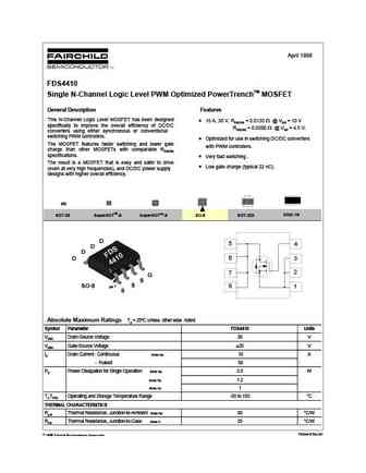
April 1998 FDS4410 Single N-Channel Logic Level PWM Optimized PowerTrenchTM MOSFET General Description FeaturesThis N-Channel Logic Level MOSFET has been designed10 A, 30 V. RDS(ON) = 0.0135 @ VGS = 10 V specifically to improve the overall efficiency of DC/DCRDS(ON) = 0.0200 @ VGS = 4.5 V.converters using either synchronous or conventional switching PWM controllers.O
9.2. Size:112K fairchild semi
fds4410a.pdf
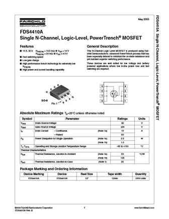
May 2005FDS4410ASingle N-Channel, Logic-Level, PowerTrench MOSFETFeatures General Description 10 A, 30 V. RDS(ON) = 13.5 m @ VGS = 10 V This N-Channel Logic Level MOSFET is produced using Fair-RDS(ON) = 20 m @ VGS = 4.5 V child Semiconductors advanced PowerTrench process that hasbeen especially tailored to minimize the on-state resistance and Fast switching speed
9.3. Size:144K fairchild semi
fds4480.pdf
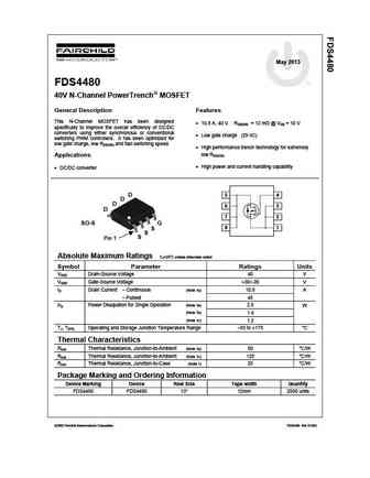
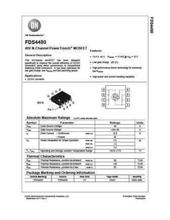
May 2013FDS4480 40V N-Channel PowerTrench MOSFET General Description Features This N-Channel MOSFET has been designed 10.8 A, 40 V. RDS(ON) = 12 m @ VGS = 10 V specifically to improve the overall efficiency of DC/DC converters using either synchronous or conventional Low gate charge (29 nC) switching PWM controllers. It has been optimized for low gate char
9.4. Size:69K fairchild semi
fds4488.pdf
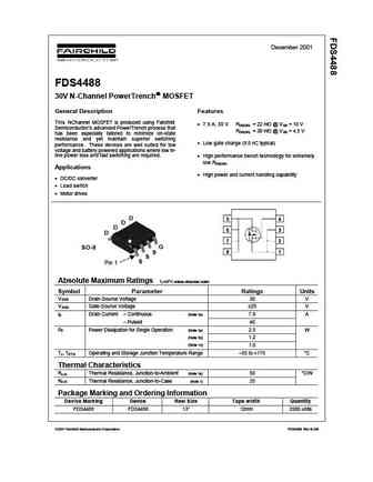
December 2001 FDS4488 30V N-Channel PowerTrench MOSFET General Description Features This N MOSFET is produced using Fairchild -Channel 7.9 A, 30 V. R = 22 m @ V = 10 V DS(ON) GSSemiconductors advanced PowerTrench process that R = 30 m @ V = 4.5 V DS(ON) GShas been especially tailored to minimize on-state resistance and yet maintain superior switching
9.5. Size:64K fairchild semi
fds4435.pdf
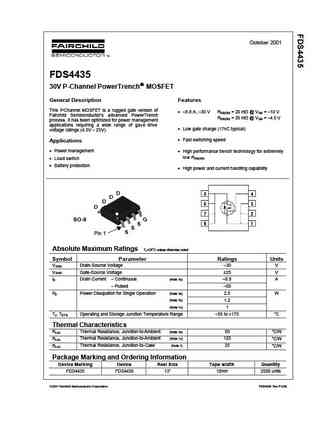
October 2001 FDS4435 30V P-Channel PowerTrench MOSFET General Description Features This P MOSFET is a rugged gate version of -Channel 8.8 A, 30 V R = 20 m @ V = 10 V DS(ON) GSFairchild Semiconductors advanced PowerTrench R = 35 m @ V = 4.5 V DS(ON) GSprocess. It has been optimized for power management applications requiring a wide range of gave
9.6. Size:296K fairchild semi
fds4435bz f085.pdf
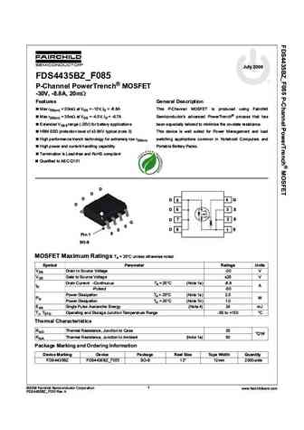
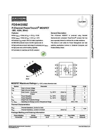
July 2009FDS4435BZ_F085P-Channel PowerTrench MOSFET -30V, -8.8A, 20m Features General Description Max rDS(on) = 20m at VGS = -10V, ID = -8.8A This P-Channel MOSFET is produced using Fairchild Max rDS(on) = 35m at VGS = -4.5V, ID = -6.7A Semiconductors advanced PowerTrench process that has Extended VGSS range (-25V) for battery applications been especially tailored to mi
9.7. Size:172K fairchild semi
fds4435a.pdf
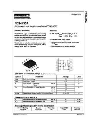
October 2001FDS4435AP-Channel Logic Level PowerTrench MOSFET General DescriptionFeaturesThis P-Channel Logic Level MOSFET is produced using -9 A, -30 V. RDS(ON) = 0.017 W @ VGS = -10 VFairchild Semiconductors advanced PowerTrench processRDS(ON) = 0.025 W @ VGS = -4.5 Vthat has been especially tailored to minimize the on-stateresistance and yet maintain low gate charg
9.8. Size:137K fairchild semi
fds4465.pdf
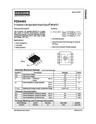
March 2003 FDS4465 P-Channel 1.8V Specified PowerTrench MOSFET General Description Features This P-Channel 1.8V specified MOSFET is a rugged 13.5 A, 20 V. RDS(ON) = 8.5 m @ VGS = 4.5 V gate version of Fairchild Semiconductors advanced RDS(ON) = 10.5 m @ VGS = 2.5 V PowerTrench process. It has been optimized for power RDS(ON) = 14 m
9.9. Size:225K fairchild semi
fds4435bz.pdf
April 2009FDS4435BZP-Channel PowerTrench MOSFET -30V, -8.8A, 20m Features General Description Max rDS(on) = 20m at VGS = -10V, ID = -8.8A This P-Channel MOSFET is produced using Fairchild Max rDS(on) = 35m at VGS = -4.5V, ID = -6.7A Semiconductors advanced PowerTrench process that has Extended VGSS range (-25V) for battery applications been especially tailored to minimi
9.10. Size:400K fairchild semi
fds4465 f085.pdf
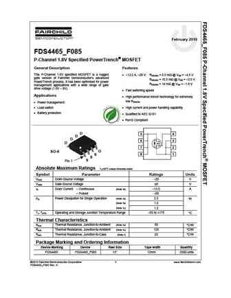
February 2010tmFDS4465_F085 P-Channel 1.8V Specified PowerTrench MOSFET General Description Features This P-Channel 1.8V specified MOSFET is a rugged 13.5 A, 20 V. RDS(ON) = 8.5 m @ VGS = 4.5 V gate version of Fairchild Semiconductors advanced RDS(ON) = 10.5 m @ VGS = 2.5 V PowerTrench process. It has been optimized for power RDS(
9.11. Size:160K onsemi
fds4480.pdf
FDS4480 40V N-Channel PowerTrench MOSFET Features General Description 10.8 A, 40 V. RDS(ON) = 12 m @ VGS = 10 VThis N-Channel MOSFET has been designed Low gate charge (29 nC)specifically to improve the overall efficiency of DC/DC converters using either synchronous or conventional High performance trench technology for extremelyswitching PWM controller
9.12. Size:264K onsemi
fds4465.pdf
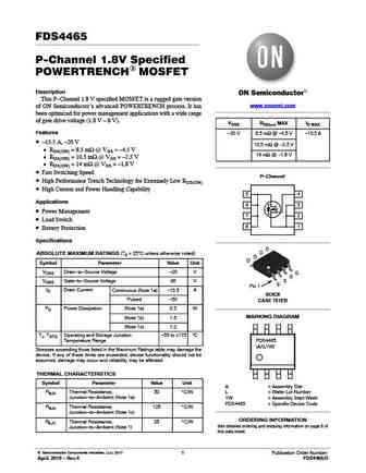
FDS4465P-Channel 1.8V SpecifiedPOWERTRENCH MOSFETDescriptionThis P-Channel 1.8 V specified MOSFET is a rugged gate versionwww.onsemi.comof ON Semiconductors advanced POWERTRENCH process. It hasbeen optimized for power management applications with a wide rangeof gate drive voltage (1.8 V 8 V).VDSS RDS(on) MAX ID MAXFeatures-20 V 8.5 mW @ -4.5 V -13.5 A 13.5
9.13. Size:342K onsemi
fds4435bz.pdf

Is Now Part ofTo learn more about ON Semiconductor, please visit our website at www.onsemi.comPlease note: As part of the Fairchild Semiconductor integration, some of the Fairchild orderable part numbers will need to change in order to meet ON Semiconductors system requirements. Since the ON Semiconductor product management systems do not have the ability to manage part nomenclatur
9.14. Size:2378K cn vbsemi
fds4435-nl.pdf
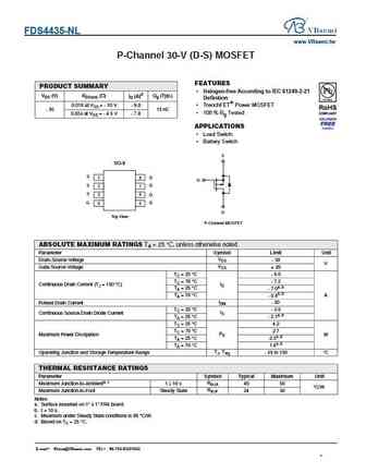
FDS4435-NLwww.VBsemi.twP-Channel 30-V (D-S) MOSFETFEATURESPRODUCT SUMMARY Halogen-free According to IEC 61249-2-21VDS (V) RDS(on) ()ID (A)d Qg (Typ.)Definition0.018 at VGS = - 10 V - 9.0 TrenchFET Power MOSFET- 30 13 nC 100 % Rg Tested0.024 at VGS = - 4.5 V - 7.8APPLICATIONS Load Switch Battery SwitchS SO-8S1 8 DG S D2 7S3 6 D
9.15. Size:812K cn vbsemi
fds4450.pdf
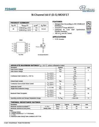
FDS4450www.VBsemi.twN-Channel 60-V (D-S) MOSFETFEATURESPRODUCT SUMMARY Halogen-free According to IEC 61249-2-21VDS (V) RDS(on) ()ID (A)d Qg (Typ.)Definition TrenchFET Power MOSFET0.025 at VGS = 10 V 7.660 10.5 nC Optimized for Low Side Synchronous0.030 at VGS = 4.5 V 6.5Rectifier Operation 100 % Rg and UIS TestedAPPLICATIONSD CCFL In
9.16. Size:819K cn vbsemi
fds4435a.pdf
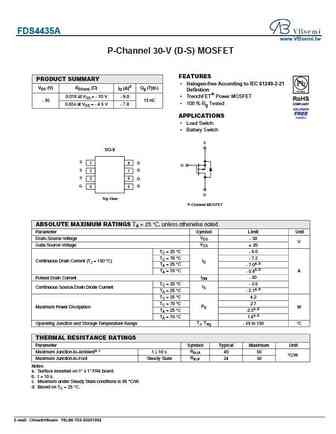
FDS4435Awww.VBsemi.twP-Channel 30-V (D-S) MOSFETFEATURESPRODUCT SUMMARY Halogen-free According to IEC 61249-2-21VDS (V) RDS(on) ()ID (A)d Qg (Typ.)Definition0.018 at VGS = - 10 V - 9.0 TrenchFET Power MOSFET- 30 13 nC 100 % Rg Tested0.024 at VGS = - 4.5 V - 7.8APPLICATIONS Load Switch Battery SwitchS SO-8S1 8 DG S D2 7S3 6 D
9.17. Size:811K cn vbsemi
fds4465-nl-9.pdf
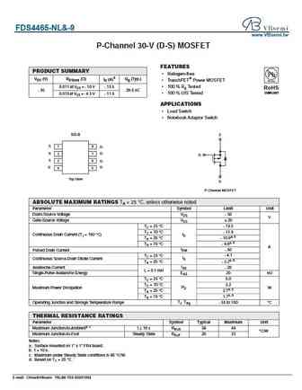
FDS4465-NL&-9www.VBsemi.twP-Channel 30-V (D-S) MOSFETFEATURESPRODUCT SUMMARY Halogen-freeVDS (V) RDS(on) ()ID (A)d Qg (Typ.) TrenchFET Power MOSFET0.011 at VGS = - 10 V - 13.5 100 % Rg TestedRoHS- 30 29.5 nCCOMPLIANT 100 % UIS Tested0.015 at VGS = - 4.5 V - 11.6APPLICATIONS Load Switch Notebook Adaptor SwitchSO-8 S S1 8 DS D2 7
9.18. Size:1468K cn vbsemi
fds4435bz.pdf
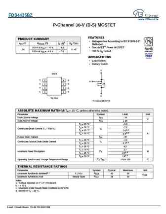
FDS4435BZwww.VBsemi.twP-Channel 30-V (D-S) MOSFETFEATURESPRODUCT SUMMARY Halogen-free According to IEC 61249-2-21VDS (V) RDS(on) ()ID (A)d Qg (Typ.)Definition0.018 at VGS = - 10 V - 9.0 TrenchFET Power MOSFET- 30 13 nC 100 % Rg Tested0.024 at VGS = - 4.5 V - 7.8APPLICATIONS Load Switch Battery SwitchS SO-8S1 8 DG S D2 7S3 6 D
Datasheet: FDS3992
, STE339S
, FDS4141
, FDS4141F085
, FDS4435BZ
, FDS4435BZF085
, FDS4465
, FDS4465F085
, 2N60
, FDS4488
, STD12L01
, FDS4501H
, STB458D
, STB440S
, FDS4559
, STB438S
, FDS4559F085
.
History: AFN1510S
Keywords - FDS4470 MOSFET datasheet
FDS4470 cross reference
FDS4470 equivalent finder
FDS4470 lookup
FDS4470 substitution
FDS4470 replacement


