2N5190 Specs and Replacement
Type Designator: 2N5190
Material of Transistor: Si
Polarity: NPN
Absolute Maximum Ratings
Maximum Collector Power Dissipation (Pc): 40 W
Maximum Collector-Base Voltage |Vcb|: 40 V
Maximum Collector-Emitter Voltage |Vce|: 40 V
Maximum Emitter-Base Voltage |Veb|: 4 V
Maximum Collector Current |Ic max|: 4 A
Max. Operating Junction Temperature (Tj): 150 °C
Electrical Characteristics
Transition Frequency (ft): 2 MHz
Forward Current Transfer Ratio (hFE), MIN: 25
Noise Figure, dB: -
Package: TO126
- BJT ⓘ Cross-Reference Search
2N5190 datasheet
..2. Size:84K onsemi
2n5190 2n5191 2n5192.pdf 

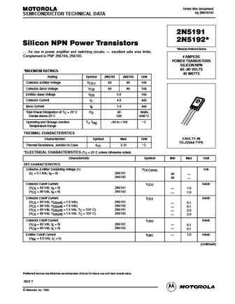
2N5190, 2N5191, 2N5192 Silicon NPN Power Transistors Silicon NPN power transistors are for use in power amplifier and switching circuits, excellent safe area limits. Complement to PNP 2N5194, 2N5195. http //onsemi.com Features ESD Ratings Machine Model, C; > 400 V 4.0 AMPERES Human Body Model, 3B; > 8000 V NPN SILICON Epoxy Meets UL 94 V-0 @ 0.125 in. POWER TRANSISTORS ... See More ⇒
..3. Size:42K jmnic
2n5190 2n5191 2n5192.pdf
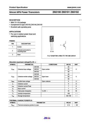
Product Specification www.jmnic.com Silicon NPN Power Transistors 2N5190 2N5191 2N5192 DESCRIPTION With TO-126 package Complement to type 2N5193,2N5194,2N5195 Excellent safe operating area APPLICATIONS For use in medium power linear and switching applications PINNING PIN DESCRIPTION 1 Emitter Collector;connected to 2 mounting base 3 Base Absolute maximum ... See More ⇒
..4. Size:118K inchange semiconductor
2n5190 2n5191 2n5192.pdf
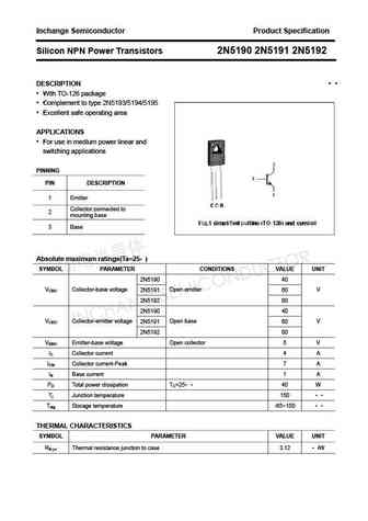
Inchange Semiconductor Product Specification Silicon NPN Power Transistors 2N5190 2N5191 2N5192 DESCRIPTION With TO-126 package Complement to type 2N5193/5194/5195 Excellent safe operating area APPLICATIONS For use in medium power linear and switching applications PINNING PIN DESCRIPTION 1 Emitter Collector;connected to 2 mounting base 3 Base Absolute max... See More ⇒
0.1. Size:84K onsemi
2n5190g.pdf

2N5190, 2N5191, 2N5192 Silicon NPN Power Transistors Silicon NPN power transistors are for use in power amplifier and switching circuits, excellent safe area limits. Complement to PNP 2N5194, 2N5195. http //onsemi.com Features ESD Ratings Machine Model, C; > 400 V 4.0 AMPERES Human Body Model, 3B; > 8000 V NPN SILICON Epoxy Meets UL 94 V-0 @ 0.125 in. POWER TRANSISTORS ... See More ⇒
0.2. Size:139K onsemi
2n5190g 2n5191g 2n5192g.pdf
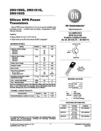
2N5190G, 2N5191G, 2N5192G Silicon NPN Power Transistors Silicon NPN power transistors are for use in power amplifier and switching circuits - excellent safe area limits. Complement to PNP http //onsemi.com 2N5194, 2N5195. 4.0 AMPERES Features NPN SILICON Epoxy Meets UL 94 V-0 @ 0.125 in. POWER TRANSISTORS These Devices are Pb-Free and are RoHS Compliant* 40, 60, 80 VOLTS -... See More ⇒
9.2. Size:212K motorola
2n5194 2n5195.pdf
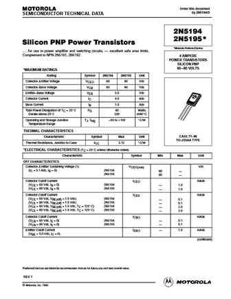
Order this document MOTOROLA by 2N5194/D SEMICONDUCTOR TECHNICAL DATA 2N5194 2N5195* Silicon PNP Power Transistors *Motorola Preferred Device . . . for use in power amplifier and switching circuits, excellent safe area limits. Complement to NPN 2N5191, 2N5192 4 AMPERE POWER TRANSISTORS ... See More ⇒
9.3. Size:230K st
2n5191 2n5192.pdf
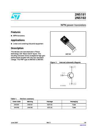
2N5191 2N5192 NPN power transistors Features NPN transistors Applications Linear and switching industrial equipment Description 1 2 The devices are manufactured in Planar 3 technology with Base Island layout. The SOT-32 resulting transistor shows exceptional high gain performance coupled with very low saturation voltage. The PNP type of 2N5192 is 2N5195. Figure ... See More ⇒
9.4. Size:206K st
2n5195.pdf
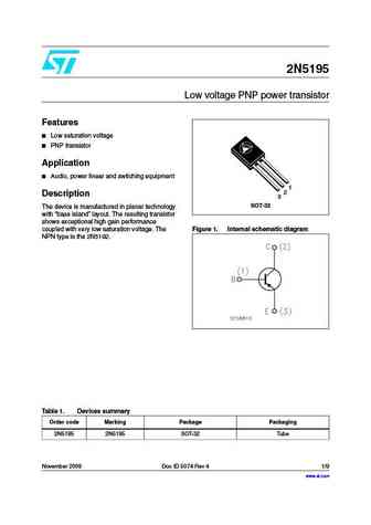
2N5195 Low voltage PNP power transistor Features Low saturation voltage PNP transistor Application Audio, power linear and switching equipment 1 2 Description 3 SOT-32 The device is manufactured in planar technology with base island layout. The resulting transistor shows exceptional high gain performance coupled with very low saturation voltage. The Figure 1.... See More ⇒
9.5. Size:65K vishay
2n5196 2n5197 2n5198 2n5199.pdf
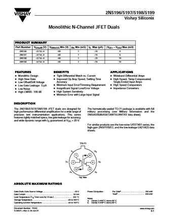
2N5196/5197/5198/5199 Vishay Siliconix Monolithic N-Channel JFET Duals PRODUCT SUMMARY Part Number VGS(off) (V) V(BR)GSS Min (V) gfs Min (mS) IG Max (pA) jVGS1 VGS2j Max (mV) 2N5196 0.7 to 4 50 1 15 5 2N5197 0.7 to 4 50 1 15 5 2N5198 0.7 to 4 50 1 15 10 2N5199 0.7 to 4 50 1 15 15 FEATURES BENEFITS APPLICATIONS D Monolithic Design D T... See More ⇒
9.6. Size:84K onsemi
2n5192g.pdf

2N5190, 2N5191, 2N5192 Silicon NPN Power Transistors Silicon NPN power transistors are for use in power amplifier and switching circuits, excellent safe area limits. Complement to PNP 2N5194, 2N5195. http //onsemi.com Features ESD Ratings Machine Model, C; > 400 V 4.0 AMPERES Human Body Model, 3B; > 8000 V NPN SILICON Epoxy Meets UL 94 V-0 @ 0.125 in. POWER TRANSISTORS ... See More ⇒
9.7. Size:84K onsemi
2n5191g.pdf
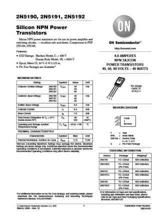
2N5190, 2N5191, 2N5192 Silicon NPN Power Transistors Silicon NPN power transistors are for use in power amplifier and switching circuits, excellent safe area limits. Complement to PNP 2N5194, 2N5195. http //onsemi.com Features ESD Ratings Machine Model, C; > 400 V 4.0 AMPERES Human Body Model, 3B; > 8000 V NPN SILICON Epoxy Meets UL 94 V-0 @ 0.125 in. POWER TRANSISTORS ... See More ⇒
9.8. Size:136K onsemi
2n5194g 2n5195g.pdf
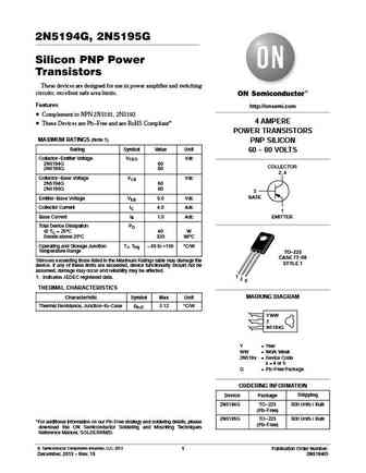
2N5194G, 2N5195G Silicon PNP Power Transistors These devices are designed for use in power amplifier and switching circuits; excellent safe area limits. Features http //onsemi.com Complement to NPN 2N5191, 2N5192 4 AMPERE These Devices are Pb-Free and are RoHS Compliant* POWER TRANSISTORS MAXIMUM RATINGS (Note 1) PNP SILICON Rating Symbol Value Unit 60 - 80 VOLTS Collecto... See More ⇒
9.9. Size:86K onsemi
2n5194 2n5195.pdf

2N5194, 2N5195 Preferred Devices Silicon PNP Power Transistors These devices are designed for use in power amplifier and switching circuits; excellent safe area limits. Complement to NPN 2N5191, 2N5192. http //onsemi.com Features Pb-Free Packages are Available* 4 AMPERE POWER TRANSISTORS MAXIMUM RATINGS (Note 1) PNP SILICON ... See More ⇒
9.10. Size:86K onsemi
2n5194g.pdf
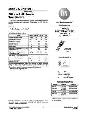
2N5194, 2N5195 Preferred Devices Silicon PNP Power Transistors These devices are designed for use in power amplifier and switching circuits; excellent safe area limits. Complement to NPN 2N5191, 2N5192. http //onsemi.com Features Pb-Free Packages are Available* 4 AMPERE POWER TRANSISTORS MAXIMUM RATINGS (Note 1) PNP SILICON ... See More ⇒
9.11. Size:86K onsemi
2n5195g.pdf

2N5194, 2N5195 Preferred Devices Silicon PNP Power Transistors These devices are designed for use in power amplifier and switching circuits; excellent safe area limits. Complement to NPN 2N5191, 2N5192. http //onsemi.com Features Pb-Free Packages are Available* 4 AMPERE POWER TRANSISTORS MAXIMUM RATINGS (Note 1) PNP SILICON ... See More ⇒
9.12. Size:130K cdil
2n5191 92.pdf
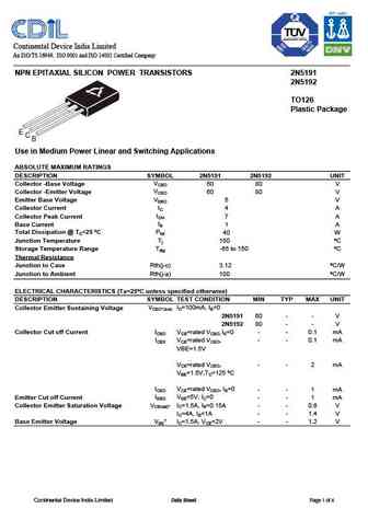
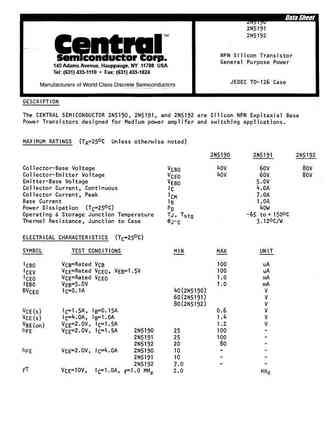
Continental Device India Limited An ISO/TS 16949, ISO 9001 and ISO 14001 Certified Company NPN EPITAXIAL SILICON POWER TRANSISTORS 2N5191 2N5192 TO126 Plastic Package E C B Use in Medium Power Linear and Switching Applications ABSOLUTE MAXIMUM RATINGS DESCRIPTION SYMBOL 2N5191 2N5192 UNIT Collector -Base Voltage VCBO 60 80 V Collector -Emitter Voltage VCEO 60 80 V Emitter Base Vo... See More ⇒
9.13. Size:42K jmnic
2n5193 2n5194 2n5195.pdf
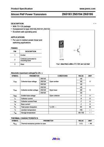
Product Specification www.jmnic.com Silicon PNP Power Transistors 2N5193 2N5194 2N5195 DESCRIPTION With TO-126 package Complement to type 2N5190,2N5191,2N5192 Excellent safe operating area APPLICATIONS For use in medium power linear and switching applications PINNING PIN DESCRIPTION 1 Emitter Collector;connected to 2 mounting base 3 Base Absolute maximum ... See More ⇒
9.14. Size:118K inchange semiconductor
2n5193 2n5194 2n5195.pdf
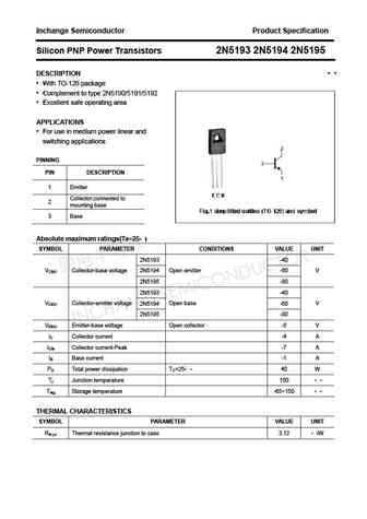
Inchange Semiconductor Product Specification Silicon PNP Power Transistors 2N5193 2N5194 2N5195 DESCRIPTION With TO-126 package Complement to type 2N5190/5191/5192 Excellent safe operating area APPLICATIONS For use in medium power linear and switching applications PINNING PIN DESCRIPTION 1 Emitter Collector;connected to 2 mounting base 3 Base Absolute max... See More ⇒
Detailed specifications: 2N5184, 2N5185, 2N5186, 2N5187, 2N5188, 2N5189, 2N518A, 2N519, 2N5401, 2N5191, 2N5192, 2N5193, 2N5194, 2N5195, 2N519A, 2N52, 2N520
Keywords - 2N5190 pdf specs
2N5190 cross reference
2N5190 equivalent finder
2N5190 pdf lookup
2N5190 substitution
2N5190 replacement