2N5629 Datasheet, Equivalent, Cross Reference Search
Type Designator: 2N5629
Material of Transistor: Si
Polarity: NPN
Maximum Collector Power Dissipation (Pc): 200 W
Maximum Collector-Base Voltage |Vcb|: 100 V
Maximum Collector-Emitter Voltage |Vce|: 100 V
Maximum Emitter-Base Voltage |Veb|: 7 V
Maximum Collector Current |Ic max|: 20 A
Max. Operating Junction Temperature (Tj): 200 °C
Transition Frequency (ft): 1 MHz
Collector Capacitance (Cc): 500 pF
Forward Current Transfer Ratio (hFE), MIN: 25
Noise Figure, dB: -
Package: TO3
2N5629 Transistor Equivalent Substitute - Cross-Reference Search
2N5629 Datasheet (PDF)
2n5629 2n5630 2n6029 2n6030.pdf

145 Adams Avenue, Hauppauge, NY 11788 USATel: (631) 435-1110 Fax: (631) 435-1824
2n5629 2n5630.pdf


Product Specification www.jmnic.com Silicon NPN Power Transistors 2N5629 2N5630 DESCRIPTION With TO-3 package Complement to type 2N6029 2N6030 APPLICATIONS For high voltage and high power amplifier applications PINNING PIN DESCRIPTION1 Base 2 Emitter3 CollectorFig.1 simplified outline (TO-3) and symbolAbsolute maximum ratings(Ta=) SYMBOL PARAMETER CONDITIO
2n5629 2n5630.pdf
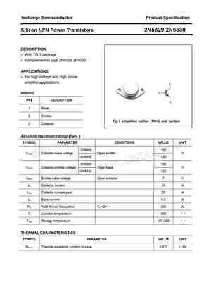

Inchange Semiconductor Product Specification Silicon NPN Power Transistors 2N5629 2N5630 DESCRIPTION With TO-3 package Complement to type 2N6029 2N6030 APPLICATIONS For high voltage and high power amplifier applications PINNING PIN DESCRIPTION1 Base 2 EmitterFig.1 simplified outline (TO-3) and symbol 3 CollectorAbsolute maximum ratings(Ta=) SYMBOL PARAMETE
2n5620.pdf

2N5620Dimensions in mm (inches). Bipolar NPN Device in a Hermetically sealed TO3 25.15 (0.99)6.35 (0.25) 26.67 (1.05)9.15 (0.36)Metal Package. 10.67 (0.42)11.18 (0.44) 1.52 (0.06)3.43 (0.135)1 2 Bipolar NPN Device. 3VCEO = 100V (case)3.84 (0.151)4.09 (0.161)7.92 (0.312) IC = 5A 12.70 (0.50) All Semelab hermetically sealed products can be processed in a
2n5623.pdf

2N5623Dimensions in mm (inches). Bipolar PNP Device in a Hermetically sealed TO3 25.15 (0.99)6.35 (0.25) 26.67 (1.05)9.15 (0.36)Metal Package. 10.67 (0.42)11.18 (0.44) 1.52 (0.06)3.43 (0.135)1 2 Bipolar PNP Device. 3VCEO = 80V (case)3.84 (0.151)4.09 (0.161)7.92 (0.312) IC = 10A 12.70 (0.50) All Semelab hermetically sealed products can be processed in a
2n5622.pdf

2N5622Dimensions in mm (inches). Bipolar NPN Device in a Hermetically sealed TO3 25.15 (0.99)6.35 (0.25) 26.67 (1.05)9.15 (0.36)Metal Package. 10.67 (0.42)11.18 (0.44) 1.52 (0.06)3.43 (0.135)1 2 Bipolar NPN Device. 3VCEO = 60V (case)3.84 (0.151)4.09 (0.161)7.92 (0.312) IC = 10A 12.70 (0.50) All Semelab hermetically sealed products can be processed in a
2n5622 2n5624 2n5626 2n5628.pdf


Product Specification www.jmnic.com Silicon NPN Power Transistors 2N5622 2N5624 2N5626 2N5628 DESCRIPTION With TO-3 package Excellent safe operating area Low collector-emitter saturation voltage APPLICATIONS For audio and general-purpose applications PINNING(see Fig.2) PIN DESCRIPTION1 Base 2 Emitter3 CollectorFig.1 simplified outline (TO-3) and symbol Abso
2n5621 2n5623 2n5625 2n5627.pdf


Product Specification www.jmnic.com Silicon PNP Power Transistors 2N5621 2N5623 2N5625 2N5627 DESCRIPTION With TO-3 package Excellent safe operating area Low collector-emitter saturation voltage APPLICATIONS For audio and general-purpose applications PINNING(see Fig.2) PIN DESCRIPTION1 Base 2 Emitter3 CollectorFig.1 simplified outline (TO-3) and symbol Abso
2n5622 2n5624 2n5626 2n5628.pdf


Inchange Semiconductor Product Specification Silicon NPN Power Transistors 2N5622 2N5624 2N5626 2N5628 DESCRIPTION With TO-3 package Excellent safe operating area Low collector saturation voltage APPLICATIONS For audio and general-purpose applications PINNING(see Fig.2) PIN DESCRIPTION1 Base 2 EmitterFig.1 simplified outline (TO-3) and symbol3 CollectorAbso
2n5621 2n5623 2n5625 2n5627.pdf


Inchange Semiconductor Product Specification Silicon PNP Power Transistors 2N5621 2N5623 2N5625 2N5627 DESCRIPTION With TO-3 package Excellent safe operating area Low collector saturation voltage APPLICATIONS For audio and general-purpose applications PINNING(see Fig.2) PIN DESCRIPTION1 Base 2 EmitterFig.1 simplified outline (TO-3) and symbol 3 CollectorAbs
2n5614 2n5616 2n5618 2n5620.pdf


Inchange Semiconductor Product Specification Silicon NPN Power Transistors 2N5614 2N5616 2N5618 2N5620 DESCRIPTION With TO-3 package Excellent safe operating area Low collector saturation voltage APPLICATIONS For general-purpose amplifier ; and switching applications PINNING(see Fig.2) PIN DESCRIPTION1 Base 2 EmitterFig.1 simplified outline (TO-3) and symbol3
Datasheet: 2N5621 , 2N5622 , 2N5623 , 2N5624 , 2N5625 , 2N5626 , 2N5627 , 2N5628 , MJE340 , 2N563 , 2N5630 , 2N5631 , 2N5632 , 2N5633 , 2N5634 , 2N5635 , 2N5636 .


