View ftx15n35g detailed specification:
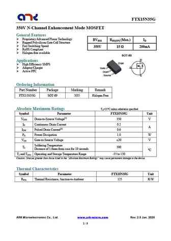
FTX15N35G 350V N-Channel Enhancement Mode MOSFET General Features Proprietary Advanced Planar Technology BVDSS RDS(ON) (Max.) ID Rugged Polysilicon Gate Cell Structure Fast Switching Speed 350V 15 200mA RoHS Compliant Halogen-free available SOT-89 D Applications Drain High Efficiency SMPS G Adaptor/Charger Gate Active PFC Drain Source S Ordering Information Part Number Package Marking Remark FTX15N35G SOT-89 N35 Halogen Free Absolute Maximum Ratings TA=25 unless otherwise specified Symbol Parameter FTX15N35G Unit VDSS Drain-to-Source Voltage[1] 350 V ID Continuous Drain Current 0.2 A IDM Pulsed Drain Current[2] 0.6 PD Power Dissipation 1.0 W VGS Gate-to-Source Voltage 20 V Soldering Temperature TL 300 Distance of 1.6mm from case for 10 seconds TJ and TSTG Operating and Storag... See More ⇒
Keywords - ALL TRANSISTORS SPECS
ftx15n35g.pdf Design, MOSFET, Power
ftx15n35g.pdf RoHS Compliant, Service, Triacs, Semiconductor
ftx15n35g.pdf Database, Innovation, IC, Electricity
