View asdm540g detailed specification:
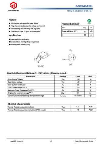
ASDM540G 100V N-Channel MOSFET Feature High density cell design for lower Rdson Product Summary Fully characterized avalanche voltage and current VDS 100 V Good stability and uniformity with high EAS Excellent package for good heat dissipation RDS(on),Typ@VGS=10V m 31 ID 33 A Application Power switching application Hard switched and High frequency circuits Uninterruptible power supply G D S TO-263 Absolute Maximum Ratings (TA=25 unless otherwise noted) Parameter Symbol Limit Unit Drain-Source Voltage 100 V VDS Gate-Source Voltage 20 V VGS Drain Current-Continuous 33 A I D Drain Current-Pulsed (Note 1) 132 A I DM 70 W Maximum Power Dissipation(Tc=25 ) P D Single pulse avalanche energy(Note 2) 96 mJ E AS Operating Junction and Storage Temperature Range -55 To 175 T ,T J STG Thermal Characteristic 1.15... See More ⇒
Keywords - ALL TRANSISTORS SPECS
asdm540g.pdf Design, MOSFET, Power
asdm540g.pdf RoHS Compliant, Service, Triacs, Semiconductor
asdm540g.pdf Database, Innovation, IC, Electricity
