View asdm60p12kq detailed specification:
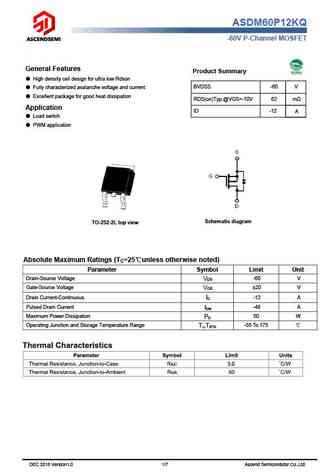
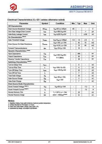
ASDM60P12KQ -60V P-Channel MOSFET General Features Product Summary High density cell design for ultra low Rdson BVDSS -60 V Fully characterized avalanche voltage and current Excellent package for good heat dissipation RDS(on)Typ.@VGS=-10V 62 m Application -12 ID A Load switch PWM application Schematic diagram TO-252-2L top view Absolute Maximum Ratings (TC=25 unless otherwise noted) Parameter Symbol Limit Unit Drain-Source Voltage -60 V VDS Gate-Source Voltage 20 V VGS Drain Current-Continuous -12 A I D Pulsed Drain Current -48 A I DM Maximum Power Dissipation 50 W P D Operating Junction and Storage Temperature Range -55 To 175 T ,T J STG 3.0 DEC 2018 Version1.0 1/7 Ascend Semicondutor Co.,Ltd ASDM60P12KQ -60V P-Channel MOSFET Electrical Characteristics (TC=25 unless otherwise noted) Parameter Symbol... See More ⇒
Keywords - ALL TRANSISTORS SPECS
asdm60p12kq.pdf Design, MOSFET, Power
asdm60p12kq.pdf RoHS Compliant, Service, Triacs, Semiconductor
asdm60p12kq.pdf Database, Innovation, IC, Electricity
