View tws6602fj detailed specification:
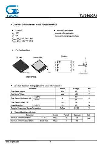
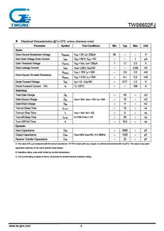
TWS6602FJ N-Channel Enhancement Mode Power MOSFET Features General Description VDS = 60V, Notebook AC-in load switch ID = 110A Battery protection charge/discharge RDS(ON) @VGS= 10V, TYP 2.9m RDS(ON) @VGS= 4.5V, TYP 4.1m Pin Configurations PDFN5*6-8L Absolute Maximum Ratings @T =25 unless otherwise noted A Parameter Symbol Ratings Unit Drain-Source Voltage VDSS 60 V Gate-Source Voltage VGSS 20 V TC=25 C 110 Drain Current (Continuous) *AC ID A TC=70 88 C Drain Current (Pulse) *B IDM 200 A Power Dissipation TC=25 C PD 83 W Operating Temperature/ Storage Temperature TJ/TSTG -55 150 Thermal Resistance Ratings Parameter Symbol Typical Maximum Unit Maximum Junction-to-Ambient t 10 s R 18 23 thJA C/W Maximum Junction-to-Case (Drain) Steady State R 1 1.5 thJC www.tw-gmc.com 1 TWS660... See More ⇒
Keywords - ALL TRANSISTORS SPECS
tws6602fj.pdf Design, MOSFET, Power
tws6602fj.pdf RoHS Compliant, Service, Triacs, Semiconductor
tws6602fj.pdf Database, Innovation, IC, Electricity
