View hy18n50w detailed specification:
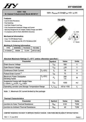
SINGLE FIG.SINGLE PHASE HALF WAVE 60Hz DERATING CURVE FIG. 2 MAXIMUM NON- T1 FORWARD CURRENT AMBIENT TEMPERATURE ( ) 1 2 5 10 1 25 50 75 10 20 150 175 0.00 0.2 0.4 0.6 4 100 125 100 HY18N50W 500V / 18A 500V, RDS(ON)=0.32W@VGS=10V, ID=9A N-Channel Enhancement Mode MOSFET Features TO-3PN Low On-State Resistance Fast Switching Low Gate Charge & Low CRSS Fully Characterized Avalanche Voltage and Current Specially Desigened for AC Adapter, Battery Charger and SMPS Drain In compliance with EU RoHs 2002/95/EC Directives 2 Mechanical Information 1 Case TO-3PN Molded Plastic 1 Gate 2 Terminals Solderable per MIL-STD-750,Method 2026 3 Source 3 Marking & Ordering Information TYPE MARKING PACKAGE PACKING HY18N50W 18N50W TO-3PN 30PCS/TUBE Absolute Maximum Ratings (TC=25 C unless otherwise specified ) Para... See More ⇒
Keywords - ALL TRANSISTORS SPECS
hy18n50w.pdf Design, MOSFET, Power
hy18n50w.pdf RoHS Compliant, Service, Triacs, Semiconductor
hy18n50w.pdf Database, Innovation, IC, Electricity
