View jmpe34n20bj datasheet:
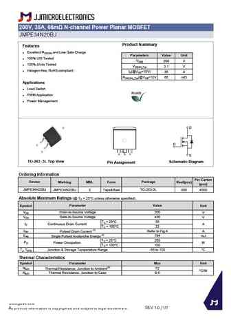
200V, 35A, 66m N-channel Power Planar MOSFETJMPE34N20BJProduct SummaryFeatures Excellent RDS(ON) and Low Gate ChargeParametersValue Unit 100% UIS TestedVDSS 200 V 100% Vds TestedVGS(th)_Typ 3.1 V Halogen-free; RoHS-compliantID(@VGS=10V) 35 ARDS(ON)_Typ(@VGS=10V 66 mWApplications Load Switch PWM Application Power ManagementDG STO-263 -3L Top ViewSchematic DiagramPin AssignmentOrdering InformationPer CartonDevice PackageMarking MSL Form Reel(pcs)(pcs)JMPE34N20BJ TO-263-3LJMPE34N20BJ 3 Tape&Reel 800 4000Absolute Maximum Ratings (@ TC = 25C unless otherwise specified)Parameter ValueSymbol UnitVDS Drain-to-Source Voltage 200 VVGS Gate-to-Source Voltage 30 VTC = 25 35CIDContinuous Drain Current ATC = 100 22CIDM Refer to Fig.4 APulsed Drain Current (1)EAS 794 mJSingle
Keywords - ALL TRANSISTORS DATASHEET
jmpe34n20bj.pdf Design, MOSFET, Power
jmpe34n20bj.pdf RoHS Compliant, Service, Triacs, Semiconductor
jmpe34n20bj.pdf Database, Innovation, IC, Electricity


LIST
Last Update
BJT: GA1A4M | SBT42 | 2SA200-Y | 2SA200-O | 2SD882-Q | 2SD882-P | 2SD882-E | 2SC945-L | 2SC945-H | 2SC4226-R23 | 2SC3357-F | 2SC3357-E | 2SC3356-R26 | 2SC3356-R24 | 2SC3356-R23 | 2SB772-Q | 2SB772-P | 2SB772-E | 2SA1015-L | 2SA1015-H | HSS8550
Popular searches
irfz44n | irf3205 | irfz44n datasheet | 2n4401 | bc547 transistor | bd139 | 2n4401 datasheet