View d882 to-251 detailed specification:
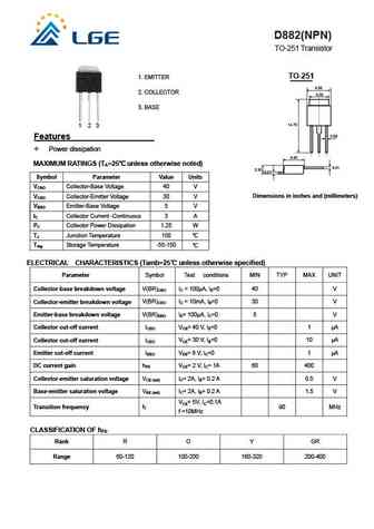
D882(NPN) TO-251 Transistor TO-251 1. EMITTER 2. COLLECTOR 3 BASE 1 2 3 Features Power dissipation MAXIMUM RATINGS (TA=25 unless otherwise noted) Symbol Parameter Value Units VCBO Collector-Base Voltage 40 V Dimensions in inches and (millimeters) VCEO Collector-Emitter Voltage 30 V VEBO Emitter-Base Voltage 5 V IC Collector Current -Continuous 3 A PC Collector Power Dissipation 1.25 W TJ Junction Temperature 150 Tstg Storage Temperature -55-150 ELECTRICAL CHARACTERISTICS (Tamb=25 unless otherwise specified) Parameter Symbol Test conditions MIN TYP MAX UNIT Collector-base breakdown voltage V(BR)CBO IC = 100 A, IE=0 40 V Collector-emitter breakdown voltage V(BR)CEO IC = 10mA, IB=0 30 V Emitter-base breakdown voltage V(BR)EBO IE= 100 A, IC=0 5 V Collector cut-off current ICBO VCB= 40 V, IE=0 1 A Collector cut-off current IC... See More ⇒
Keywords - ALL TRANSISTORS SPECS
d882 to-251.pdf Design, MOSFET, Power
d882 to-251.pdf RoHS Compliant, Service, Triacs, Semiconductor
d882 to-251.pdf Database, Innovation, IC, Electricity
