View buk581-100a 2 datasheet:
POWER MOSFET, IGBT, IC, TRIACS DATABASE. Electronic Supply. INNOVATION CATALOG
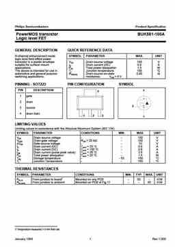
Philips Semiconductors Product Specification PowerMOS transistor BUK581-100A Logic level FET GENERAL DESCRIPTION QUICK REFERENCE DATA N-channel enhancement mode SYMBOL PARAMETER MAX. UNIT logic level field-effect power transistor in a plastic envelope VDS Drain-source voltage 100 V suitable for surface mount ID Drain current (DC) 0.9 A applications. Ptot Total power dissipation 1.5 W The device is intended for use in Tj Junction temperature 150 ?C automotive and general purpose RDS(ON) Drain-source on-state 0.90 ? switching applications. resistance; VGS = 5 V PINNING - SOT223 PIN CONFIGURATION SYMBOL PIN DESCRIPTION d 4 1 gate 2 drain g 3 source 4 drain (tab) 1 2 3 s LIMITING VALUES Limiting values in accordance with the Absolute Maximum System (IEC 134) SYMBOL P
Keywords
buk581-100a 2 Datasheet, Design, MOSFET, Power
buk581-100a 2 RoHS, Compliant, Service, Triacs, Semiconductor
buk581-100a 2 Database, Innovation, IC, Electricity


LIST
Last Update
BJT: SBT42 | 2SA200-Y | 2SA200-O | 2SD882-Q | 2SD882-P | 2SD882-E | 2SC945-L | 2SC945-H | 2SC4226-R23 | 2SC3357-F | 2SC3357-E | 2SC3356-R26 | 2SC3356-R24 | 2SC3356-R23 | 2SB772-Q | 2SB772-P | 2SB772-E | 2SA1015-L | 2SA1015-H | HSS8550 | HSS8050
Popular searches
irfz44n | irf3205 | irfz44n datasheet | 2n4401 | bc547 transistor | bd139 | 2n4401 datasheet