asdm30p100kq.pdf Principales características:
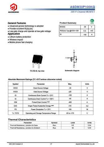
ASDM30P100KQ -30V P-Channel MOSFET Product Summary General Features Advanced groove technology is adopted BVDSS -30 V Provide excellent R DS(ON) RDS(on).Typ.@VGS=-10V m 5.0 Low gate charge and operate at low gate voltage Application ID -100 A Lithium battery protection Wireless impact Mobile phone fast charging Schematic diagram TO-252-2L top view Absolute Maximum Ratings (TC=25 unless otherwise noted) Symbol Parameter Max. Units VDSS Drain-Source Voltage -30 V VGSS Gate-Source Voltage 20 V ID Continuous Drain Current T = 25 -100 A C ID Continuous Drain Current T = 100 -59 A C IDM Pulsed Drain Current note1 -400 A EAS Single Pulsed Avalanche Energy note2 210 mJ PD Power Dissipation T = 25 109 W C TJ, TSTG Operating and Storage Temperature Range -55 to +175 3.0 DEC 2018 Version1.0 1/7 Ascend Semicondut
Keywords - ALL TRANSISTORS. Principales características
asdm30p100kq.pdf Design, MOSFET, Power
asdm30p100kq.pdf RoHS Compliant, Service, Triacs, Semiconductor
asdm30p100kq.pdf Database, Innovation, IC, Electricity
🌐 : EN ES РУ

Liste
Recientemente añadidas las descripciónes de los transistores:
BJT: GA1A4M | SBT42 | 2SA200-Y | 2SA200-O | 2SD882-Q | 2SD882-P | 2SD882-E | 2SC945-L | 2SC945-H | 2SC4226-R23 | 2SC3357-F | 2SC3357-E | 2SC3356-R26 | 2SC3356-R24 | 2SC3356-R23 | 2SB772-Q | 2SB772-P | 2SB772-E | 2SA1015-L | 2SA1015-H | HSS8550
Popular searches
irfz44n | irf3205 | irfz44n datasheet | 2n4401 | bc547 transistor | bd139 | 2n4401 datasheet