IPP111N15N3 MOSFET Equivalente. Reemplazo. Hoja de especificaciones. Principales características
Número de Parte: IPP111N15N3
Tipo de FET: MOSFET
Polaridad de transistor: N
ESPECIFICACIONES MÁXIMAS
Pdⓘ - Máxima disipación de potencia: 214 W|Vds|ⓘ - Voltaje máximo drenador - fuente: 150 V
|Vgs|ⓘ - Voltaje máximo fuente - puerta: 20 V
|Id|ⓘ - Corriente continua de drenaje: 83 A
Tjⓘ - Temperatura máxima de unión: 175 °C
CARACTERÍSTICAS ELÉCTRICAS
trⓘ - Tiempo de subida: 35 nS
Cossⓘ - Capacitancia de salida: 378 pF
Rds(on)ⓘ - Resistencia estado encendido drenaje a fuente: 0.0111 Ohm
Paquete / Cubierta: TO220
Búsqueda de reemplazo de IPP111N15N3 MOSFET
IPP111N15N3 PDF Specs
ipp111n15n3.pdf

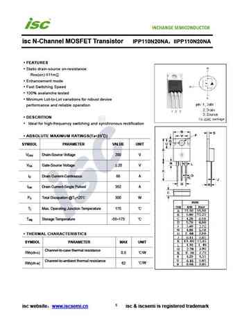
isc N-Channel MOSFET Transistor IPP111N15N3 IIPP111N15N3 FEATURES Static drain-source on-resistance RDS(on) 11.1m Enhancement mode Fast Switching Speed 100% avalanche tested Minimum Lot-to-Lot variations for robust device performance and reliable operation DESCRITION Ideal for high-frequency switching and synchronous rectification ABSOLUTE MAXIMUM RATINGS(T... See More ⇒
ipb108n15n3g ipp111n15n3g ipi111n15n3g.pdf
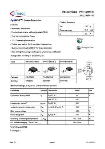
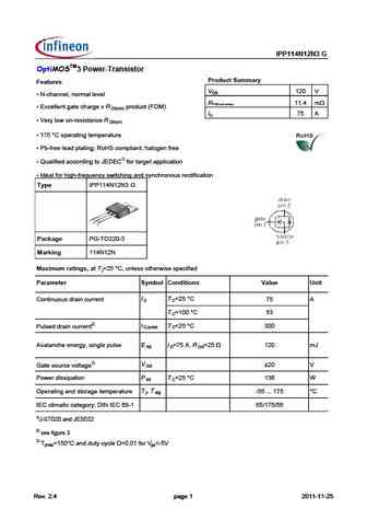
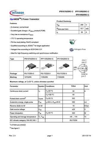
IPB108N15N3 G IPP111N15N3 G IPI111N15N3 G OptiMOSTM3 Power-Transistor Product Summary Features VDS 150 V N-channel, normal level RDS(on),max (TO263) 10.8 mW Excellent gate charge x R product (FOM) DS(on) ID 83 A Very low on-resistance R DS(on) 175 C operating temperature Pb-free lead plating; RoHS compliant; Halogen free Qualified according to JEDE... See More ⇒
ipb108n15n3-g ipp111n15n3-g ipi111n15n3-g.pdf
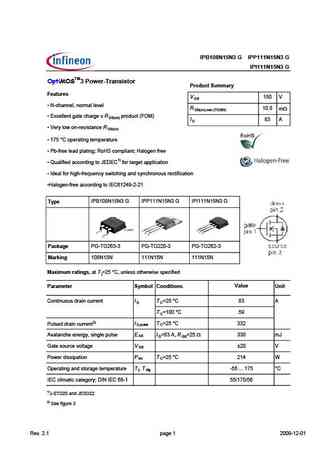
IPB108N15N3 G IPP111N15N3 G IPI111N15N3 G OptiMOSTM3 Power-Transistor Product Summary Features V 150 V DS N-channel, normal level R 10.8 m DS(on),max (TO263) Excellent gate charge x R product (FOM) DS(on) I 83 A D Very low on-resistance R DS(on) 175 C operating temperature Pb-free lead plating; RoHS compliant; Halogen free Qualified according to JE... See More ⇒
ipb114n03l-g ipp114n03l-g.pdf
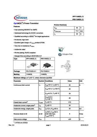
Type IPP114N03L G IPB114N03L G OptiMOS 3 Power-Transistor Product Summary Features V 30 V DS Fast switching MOSFET for SMPS R 11.4 m DS(on),max Optimized technology for DC/DC converters I 30 A D Qualified according to JEDEC1) for target applications N-channel, logic level Excellent gate charge x R product (FOM) DS(on) Very low on-resistance R DS(on... See More ⇒


Otros transistores... IPP05CN10N , IPP070N08N3 , IPP075N15N3 , IPP076N12N3 , IPP076N15N5 , IPP093N06N3 , IPP100N08N3 , IPP110N20N3 , IRLB4132 , IPP114N12N3 , IPP12CN10L , IPP147N12N3 , IPP16CN10N , IPP200N15N3 , IPP200N25N3 , IPP320N20N3 , IPP530N15N3 .


Liste
Recientemente añadidas las descripciónes de los transistores:
MOSFET: AP3N50K | AP3N50F | AP3912GD | AP3415E | AP3404S | AP3404 | AP3205 | AP3139 | AP3134N5 | AP3101A | AP3100A | AP30P06K | AP30P06 | AP30N04K | AP30N03K | AP30H80K
Popular searches
k3599 transistor datasheet | 2sc1735 | transistor 2sc5200 | 2sb560 transistor | a1273 | c3421 transistor | c644 transistor | fgpf4536 datasheet