ftk4015d.pdf Principales características:
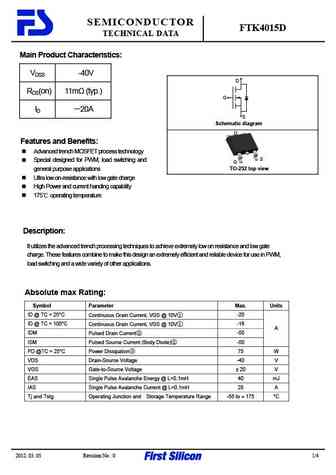
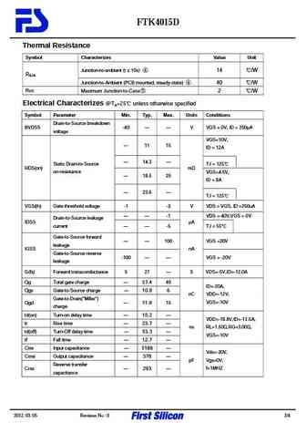
SEMICONDUCTOR FTK4015D TECHNICAL DATA Main Product Characteristics VDSS -40V D RDS(on) 11m (typ.) G ID 20A S Schematic diagram D Features and Benefits Advanced trench MOSFET process technology S Special designed for PWM, load switching and G TO-252 top view general purpose applications Ultra low on-resistance with low gate charge High Power and current handing capability 175 operating temperature Description It utilizes the advanced trench processing techniques to achieve extremely low on resistance and low gate charge. These features combine to make this design an extremely efficient and reliable device for use in PWM, load switching and a wide variety of other applications. Absolute max Rating Symbol Parameter Max. Units ID @ TC = 25 C -20 Continuous Drain Current, VGS @ 10V ID @ TC = 100 C -16 Continuous Dra
Keywords - ALL TRANSISTORS. Principales características
ftk4015d.pdf Design, MOSFET, Power
ftk4015d.pdf RoHS Compliant, Service, Triacs, Semiconductor
ftk4015d.pdf Database, Innovation, IC, Electricity
🌐 : EN ES РУ

Liste
Recientemente añadidas las descripciónes de los transistores:
BJT: GA1A4M | SBT42 | 2SA200-Y | 2SA200-O | 2SD882-Q | 2SD882-P | 2SD882-E | 2SC945-L | 2SC945-H | 2SC4226-R23 | 2SC3357-F | 2SC3357-E | 2SC3356-R26 | 2SC3356-R24 | 2SC3356-R23 | 2SB772-Q | 2SB772-P | 2SB772-E | 2SA1015-L | 2SA1015-H | HSS8550
Popular searches
irfz44n | irf3205 | irfz44n datasheet | 2n4401 | bc547 transistor | bd139 | 2n4401 datasheet