r07ds0296ej rqj0304dqd.pdf Principales características:
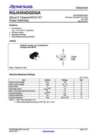
Preliminary Datasheet RQJ0304DQDQA R07DS0296EJ0200 (Previous REJ03G1717-0100) Silicon P Channel MOS FET Rev.2.00 Power Switching Mar 28, 2011 Features Low gate drive VDSS 30 V and 2.5 V gate drive Low drive current High speed switching Small traditional package (MPAK) Outline RENESAS Package code PLSP0003ZB-A (Package name MPAK) 3 D 3 2 1. Source G 1 2. Gate 3. Drain 2 S 1 Notes Marking is "DQ". Absolute Maximum Ratings (Ta = 25 C) Item Symbol Ratings Unit Drain to source voltage VDSS 30 V Gate to source voltage VGSS +8 / 12 V Drain current ID 1.8 A Drain peak current ID(pulse) Note1 8 A Body - drain diode reverse drain current IDR 1.8 A Channel dissipation Pch Note2 0.8 W Channel temperature Tch 150 C Storage temperature Tstg 55 to +150 C Notes 1. PW 10 s, Duty cycle 1%
Keywords - ALL TRANSISTORS. Principales características
r07ds0296ej rqj0304dqd.pdf Design, MOSFET, Power
r07ds0296ej rqj0304dqd.pdf RoHS Compliant, Service, Triacs, Semiconductor
r07ds0296ej rqj0304dqd.pdf Database, Innovation, IC, Electricity
🌐 : EN ES РУ

Liste
Recientemente añadidas las descripciónes de los transistores:
BJT: GA1A4M | SBT42 | 2SA200-Y | 2SA200-O | 2SD882-Q | 2SD882-P | 2SD882-E | 2SC945-L | 2SC945-H | 2SC4226-R23 | 2SC3357-F | 2SC3357-E | 2SC3356-R26 | 2SC3356-R24 | 2SC3356-R23 | 2SB772-Q | 2SB772-P | 2SB772-E | 2SA1015-L | 2SA1015-H | HSS8550
Popular searches
irfz44n | irf3205 | irfz44n datasheet | 2n4401 | bc547 transistor | bd139 | 2n4401 datasheet