2n7002w.pdf datasheet:
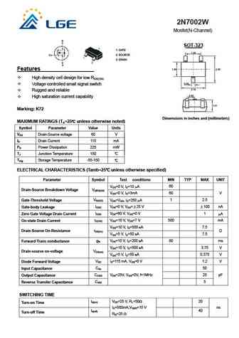
2N7002W Mosfet(N-Channel)SOT-3231. GATE 2. SOURCE 3. DRAIN Features High density cell design for low RDS(ON) Voltage controlled small signal switch Rugged and reliable High saturation current capability Marking: K72 Dimensions in inches and (millimeters)MAXIMUM RATINGS (TA=25 unless otherwise noted) Symbol Parameter Value UnitsVDS Drain-Source voltage 60 V ID Drain Current 115 mA PD Power Dissipation 225 mW TJ Junction Temperature 150 Tstg Storage Temperature -55-150 ELECTRICAL CHARACTERISTICS (Tamb=25 unless otherwise specified) Parameter Symbol Test conditions MIN TYP MAX UNITVGS=0 V, ID=10 A 60Drain-Source Breakdown Voltage V(BR)DSSVGS=0 V, ID=3mA 60 V Gate-Threshold Voltage Vth(GS) VDS=VGS, ID=250 A 1 2.5Gate-body Leakage lGSS VDS=0 V, VGS=25 V 100 nA Zero Gate Voltage Drain Current IDSS VDS=60 V, V
Keywords - ALL TRANSISTORS DATASHEET
2n7002w.pdf Design, MOSFET, Power
2n7002w.pdf RoHS Compliant, Service, Triacs, Semiconductor
2n7002w.pdf Database, Innovation, IC, Electricity


Liste
Recientemente añadidas las descripciónes de los transistores:
BJT: GA1A4M | SBT42 | 2SA200-Y | 2SA200-O | 2SD882-Q | 2SD882-P | 2SD882-E | 2SC945-L | 2SC945-H | 2SC4226-R23 | 2SC3357-F | 2SC3357-E | 2SC3356-R26 | 2SC3356-R24 | 2SC3356-R23 | 2SB772-Q | 2SB772-P | 2SB772-E | 2SA1015-L | 2SA1015-H | HSS8550
Popular searches
irfz44n | irf3205 | irfz44n datasheet | 2n4401 | bc547 transistor | bd139 | 2n4401 datasheet