g110n06 to252.pdf datasheet:
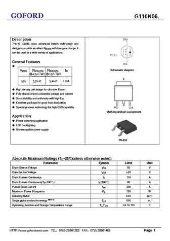
GOFORDG110N06.Description The G110N06. uses advanced trench technology and design to provide excellent R with low gate charge. It DS(ON) can be used in a wide variety of applications. General Features Schematic diagram VDSS RDS(ON) RDS(ON) ID @4.5V (Typ) @ 10V (Typ)m m 11055V 5.8 5.4 A High density cell design for ultra low Rdson Fully characterized avalanche voltage and current Good stability and uniformity with high EAS Excellent package for good heat dissipation Special process technology for high ESD capability Marking and pin assignment Application Power switching application LED backlighting Uninterruptible power supply TO-252Absolute Maximum Ratings (TC=25unless otherwise noted) Parameter Symbol Limit Unit Drain-Source Voltage 55 V VDS Gate-Source Voltage 2
Keywords - ALL TRANSISTORS DATASHEET
g110n06 to252.pdf Design, MOSFET, Power
g110n06 to252.pdf RoHS Compliant, Service, Triacs, Semiconductor
g110n06 to252.pdf Database, Innovation, IC, Electricity


Liste
Recientemente añadidas las descripciónes de los transistores:
BJT: GA1A4M | SBT42 | 2SA200-Y | 2SA200-O | 2SD882-Q | 2SD882-P | 2SD882-E | 2SC945-L | 2SC945-H | 2SC4226-R23 | 2SC3357-F | 2SC3357-E | 2SC3356-R26 | 2SC3356-R24 | 2SC3356-R23 | 2SB772-Q | 2SB772-P | 2SB772-E | 2SA1015-L | 2SA1015-H | HSS8550
Popular searches
irfz44n | irf3205 | irfz44n datasheet | 2n4401 | bc547 transistor | bd139 | 2n4401 datasheet