j210.pdf datasheet:

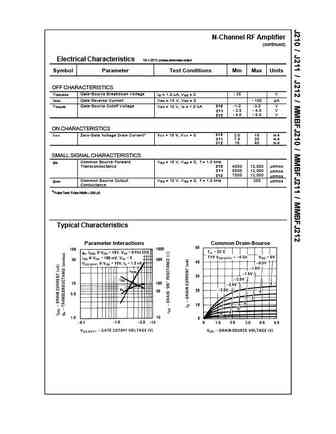
J210 MMBFJ210J211 MMBFJ211J212 MMBFJ212GSG TO-92S SOT-23D NOTE: Source & DrainDMark: 62V / 62W / 62X are interchangeableN-Channel RF AmplifierThis device is designed for HF/VHF mixer/amplifier andapplications where Process 50 is not adequate. Sufficientgain and low noise for sensitive receivers. Sourced fromProcess 90.Absolute Maximum Ratings* TA = 25C unless otherwise notedSymbol Parameter Value UnitsVDG Drain-Gate Voltage 25 VVGS Gate-Source Voltage - 25 VIGF Forward Gate Current 10 mA5Operating and Storage Junction Temperature Range -55 to +150TJ ,Tstg C*These ratings are limiting values above which the serviceability of any semiconductor device may be impaired.NOTES:1) These ratings are based on a maximum junction temperature of 150 degrees C.2) These are steady state limits. The factory should be consulted on applications in
Keywords - ALL TRANSISTORS DATASHEET
j210.pdf Design, MOSFET, Power
j210.pdf RoHS Compliant, Service, Triacs, Semiconductor
j210.pdf Database, Innovation, IC, Electricity


Liste
Recientemente añadidas las descripciónes de los transistores:
BJT: GA1A4M | SBT42 | 2SA200-Y | 2SA200-O | 2SD882-Q | 2SD882-P | 2SD882-E | 2SC945-L | 2SC945-H | 2SC4226-R23 | 2SC3357-F | 2SC3357-E | 2SC3356-R26 | 2SC3356-R24 | 2SC3356-R23 | 2SB772-Q | 2SB772-P | 2SB772-E | 2SA1015-L | 2SA1015-H | HSS8550
Popular searches
irfz44n | irf3205 | irfz44n datasheet | 2n4401 | bc547 transistor | bd139 | 2n4401 datasheet