View btd965n3 datasheet:
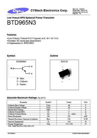
Spec. No. C847N3 Issued Date 2003.07.02 CYStech Electronics Corp. Revised Date 2013.01.03 Page No. 1/6 Low Vcesat NPN Epitaxial Planar Transistor BTD965N3 Features Low VCE(sat), VCE(sat)=0.35 V (typical), at IC / IB = 3A / 0.1A Excellent DC current gain characteristics Complementary to BTB1386N3 Symbol Outline BTD965N3 SOT-23 B Base C Collector E Emitter Absolute Maximum Ratings (Ta=25 C) Parameter Symbol Limits Unit Collector-Base Voltage VCBO 40 V Collector-Emitter Voltage VCEO 20 V Emitter-Base Voltage VEBO 7 V Collector Current (DC) IC 5 A Collector Current (Pulse) ICP 8 (Note ) A Power Dissipation Pd 225 mW Thermal Resistance, Junction to Ambient R JA 556 C/W Junction Temperature Tj 150 C Storage Temperature Tstg -55 +150 C Note Single Pulse Pw 350 s, Duty 2%. BTD2098N3 CYStek Product Sp
Keywords - ALL TRANSISTORS DATASHEET
btd965n3.pdf Design, MOSFET, Power
btd965n3.pdf RoHS Compliant, Service, Triacs, Semiconductor
btd965n3.pdf Database, Innovation, IC, Electricity


LIST
Last Update
BJT: GA1A4M | SBT42 | 2SA200-Y | 2SA200-O | 2SD882-Q | 2SD882-P | 2SD882-E | 2SC945-L | 2SC945-H | 2SC4226-R23 | 2SC3357-F | 2SC3357-E | 2SC3356-R26 | 2SC3356-R24 | 2SC3356-R23 | 2SB772-Q | 2SB772-P | 2SB772-E | 2SA1015-L | 2SA1015-H | HSS8550
Popular searches
irfz44n | irf3205 | irfz44n datasheet | 2n4401 | bc547 transistor | bd139 | 2n4401 datasheet