View tmp20n50 tmpf20n50 datasheet:
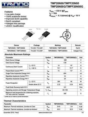
TMP20N50/TMPF20N50 TMP20N50G/TMPF20N50G VDSS = 550 V @Tjmax Features ID = 18A Low gate charge RDS(on) = 0.3 W(max) @ VGS= 10 V 100% avalanche tested Improved dv/dt capability RoHS compliant Halogen free package JEDEC Qualification D G S Device Package Marking Remark TMP20N50 / TMPF20N50 TO-220 / TO-220F TMP20N50 / TMPF20N50 RoHS TMP20N50G / TMPF20N50G TO-220 / TO-220F TMP20N50G / TMPF20N50G Halogen Free Absolute Maximum Ratings Parameter Symbol TMP20N50(G) TMPF20N50(G) Unit Drain-Source Voltage VDS 500 V Gate-Source Voltage VGS 30 V TC = 25 18 18* A Continuous Drain Current ID TC = 100 13.1 13.1* A Pulsed Drain Current (Note 1) IDM 72 72* A Single Pulse Avalanche Energy (Note 2) EAS 954 mJ Repetitive Avalanche Current (Note 1) IAR 18 A Repetitive Avalanche Energy (Note 1) EAR 29 mJ TC = 25
Keywords - ALL TRANSISTORS DATASHEET
tmp20n50 tmpf20n50.pdf Design, MOSFET, Power
tmp20n50 tmpf20n50.pdf RoHS Compliant, Service, Triacs, Semiconductor
tmp20n50 tmpf20n50.pdf Database, Innovation, IC, Electricity


LIST
Last Update
BJT: GA1A4M | SBT42 | 2SA200-Y | 2SA200-O | 2SD882-Q | 2SD882-P | 2SD882-E | 2SC945-L | 2SC945-H | 2SC4226-R23 | 2SC3357-F | 2SC3357-E | 2SC3356-R26 | 2SC3356-R24 | 2SC3356-R23 | 2SB772-Q | 2SB772-P | 2SB772-E | 2SA1015-L | 2SA1015-H | HSS8550
Popular searches
irfz44n | irf3205 | irfz44n datasheet | 2n4401 | bc547 transistor | bd139 | 2n4401 datasheet