View ced4301 ceu4301 detailed specification:
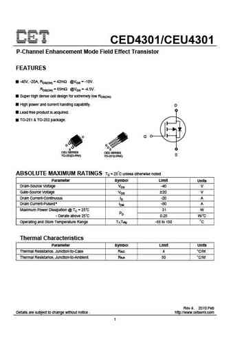
CED4301/CEU4301 P-Channel Enhancement Mode Field Effect Transistor FEATURES -40V, -20A, RDS(ON) = 42m @VGS = -10V. RDS(ON) = 65m @VGS = -4.5V. Super high dense cell design for extremely low RDS(ON). High power and current handing capability. D Lead free product is acquired. TO-251 & TO-252 package. D G G S CEU SERIES CED SERIES S TO-252(D-PAK) TO-251(I-PAK) ABSOLUTE MAXIMUM RATINGS Tc = 25 C unless otherwise noted Parameter Symbol Limit Units Drain-Source Voltage VDS -40 V Gate-Source Voltage VGS 20 V Drain Current-Continuous ID -20 A Drain Current-Pulsed a IDM -80 A Maximum Power Dissipation @ TC = 25 C 31 W PD - Derate above 25 C 0.25 W/ C Operating and Store Temperature Range TJ,Tstg -55 to 150 C Thermal Characteristics Parameter Symbol Limit Units Thermal Resistance, Junction-to-Case R JC 4 C/W Thermal Resistance, Junction-to-Ambient R JA ... See More ⇒
Keywords - ALL TRANSISTORS SPECS
ced4301 ceu4301.pdf Design, MOSFET, Power
ced4301 ceu4301.pdf RoHS Compliant, Service, Triacs, Semiconductor
ced4301 ceu4301.pdf Database, Innovation, IC, Electricity
