View 2n7002kw detailed specification:
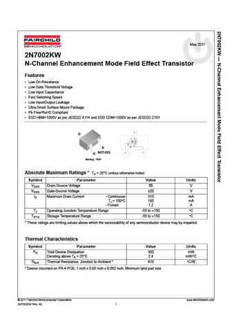
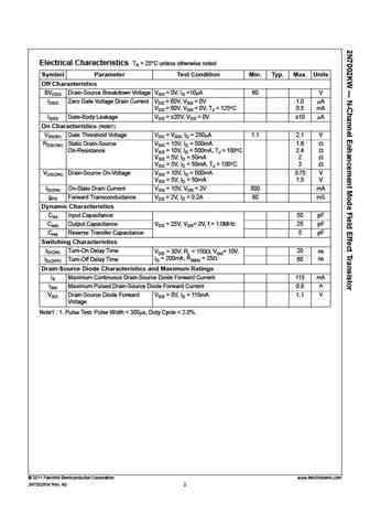
May 2011 2N7002KW N-Channel Enhancement Mode Field Effect Transistor Features Low On-Resistance Low Gate Threshold Voltage Low Input Capacitance Fast Switching Speed Low Input/Output Leakage Ultra-Small Surface Mount Package Pb Free/RoHS Compliant ESD HBM=1000V as per JESD22 A114 and ESD CDM=1500V as per JESD22 C101 D S SOT-323 G Marking 7KW Absolute Maximum Ratings * TA = 25 C unless otherwise noted Symbol Parameter Value Units VDSS Drain-Source Voltage 60 V VGSS Gate-Source Voltage 20 V ID Maximum Drain Current - Continuous 310 mA TJ = 100 C 195 mA - Pulsed 1.2 A TJ Operating Junction Temperature Range -55 to +150 C TSTG Storage Temperature Range -55 to +150 C * These ratings are limiting values above which the serviceability of any semiconductor device may by impaired. Thermal Characteristics Symbol Parameter Va... See More ⇒
Keywords - ALL TRANSISTORS SPECS
2n7002kw.pdf Design, MOSFET, Power
2n7002kw.pdf RoHS Compliant, Service, Triacs, Semiconductor
2n7002kw.pdf Database, Innovation, IC, Electricity
