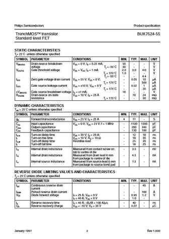
View buk7524-55 3 detailed specification:
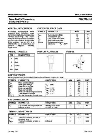
Philips Semiconductors Product specification TrenchMOS transistor BUK7524-55 Standard level FET GENERAL DESCRIPTION QUICK REFERENCE DATA N-channel enhancement mode SYMBOL PARAMETER MAX. UNIT standard level field-effect power transistor in a plastic envelope using VDS Drain-source voltage 55 V trench technology. The device ID Drain current (DC) 45 A features very low on-state resistance Ptot Total power dissipation 103 W and has integral zener diodes giving Tj Junction temperature 175 C ESD protection up to 2kV. It is RDS(ON) Drain-source on-state 24 m intended for use in automotive and resistance VGS = 10 V general purpose switching applications. PINNING - TO220AB PIN CONFIGURATION SYMBOL PIN DESCRIPTION d tab 1 gate 2 drain g 3 source tab drain s 1 2 3 LIMITING VALUES Limiting values in accordance with the Absolute Maximum System (IEC 134) S... See More ⇒
Keywords - ALL TRANSISTORS SPECS
buk7524-55 3.pdf Design, MOSFET, Power
buk7524-55 3.pdf RoHS Compliant, Service, Triacs, Semiconductor
buk7524-55 3.pdf Database, Innovation, IC, Electricity


