View pk618ba detailed specification:
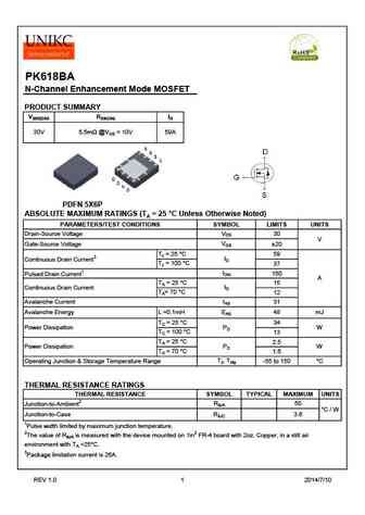
PK618BA N-Channel Enhancement Mode MOSFET PRODUCT SUMMARY V(BR)DSS RDS(ON) ID 5.5m @VGS = 10V 30V 59A PDFN 5X6P ABSOLUTE MAXIMUM RATINGS (TA = 25 C Unless Otherwise Noted) PARAMETERS/TEST CONDITIONS SYMBOL LIMITS UNITS VDS Drain-Source Voltage 30 V VGS Gate-Source Voltage 20 Tc = 25 C 59 ID Continuous Drain Current3 Tc = 100 C 37 IDM 150 Pulsed Drain Current1 A TA = 25 C 15 ID Continuous Drain Current TA= 70 C 12 IAS Avalanche Current 31 EAS Avalanche Energy L =0.1mH 48 mJ TC = 25 C 34 PD Power Dissipation W TC = 100 C 13 TA = 25 C 2.5 PD Power Dissipation W TA = 70 C 1.6 TJ, Tstg Operating Junction & Storage Temperature Range -55 to 150 C THERMAL RESISTANCE RATINGS THERMAL RESISTANCE SYMBOL TYPICAL MAXIMUM UNITS RqJA 50 Junction-to-Ambient2 C / W Junction-to-Case RqJC 3.6 1 Pulse widt... See More ⇒
Keywords - ALL TRANSISTORS SPECS
pk618ba.pdf Design, MOSFET, Power
pk618ba.pdf RoHS Compliant, Service, Triacs, Semiconductor
pk618ba.pdf Database, Innovation, IC, Electricity


LIST
Last Update
BJT: GA1A4M | SBT42 | 2SA200-Y
Popular searches
irfz44n | irf3205 | irfz44n datasheet | 2n4401 | bc547 transistor | bd139 | 2n4401 datasheet