View 2n2609 datasheet:
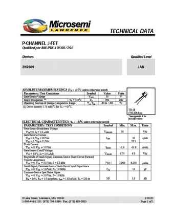
TECHNICAL DATA P-CHANNEL J-FET Qualified per MIL-PRF-19500/296 Devices Qualified Level 2N2609 JAN ABSOLUTE MAXIMUM RATINGS (T = +250C unless otherwise noted) A Parameters / Test Conditions Symbol Value Units Gate-Source Voltage V 30 V GSS(1)Power Dissipation T = +250C P 300 mW A D0Operating Junction & Storage Temperature Range Top Tstg -65 to +200 C , (1) Derate linearly 1.71 mW/0C for T > +250C. A TO-18 (TO-206AA) *See appendix A for package outline ELECTRICAL CHARACTERISTICS (T = +250C unless otherwise noted) APARAMETERS / TEST CONDITIONS Symbol Min. Max. Units Gate-Source Breakdown Voltage V = 0, I = 1.0 Adc V 30 Vdc DS G (BR)GSSGate Reverse Current VDS = 0, VGS = 30 Vdc IGSS 30 Adc VDS = 0, VGS = 15 Vdc 22.5 Drain Current V = 0, V = 5.0 Vdc I -2.0 -10.0 mAdc GS DS DDSSGate-Source Cutoff Voltage V =
Keywords - ALL TRANSISTORS DATASHEET
2n2609.pdf Design, MOSFET, Power
2n2609.pdf RoHS Compliant, Service, Triacs, Semiconductor
2n2609.pdf Database, Innovation, IC, Electricity


LIST
Last Update
BJT: GA1A4M | SBT42 | 2SA200-Y | 2SA200-O | 2SD882-Q | 2SD882-P | 2SD882-E | 2SC945-L | 2SC945-H | 2SC4226-R23 | 2SC3357-F | 2SC3357-E | 2SC3356-R26 | 2SC3356-R24 | 2SC3356-R23 | 2SB772-Q | 2SB772-P | 2SB772-E | 2SA1015-L | 2SA1015-H | HSS8550
Popular searches
irfz44n | irf3205 | irfz44n datasheet | 2n4401 | bc547 transistor | bd139 | 2n4401 datasheet