View 2n7000bu datasheet:
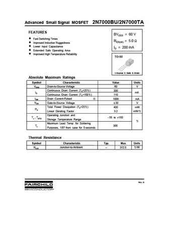
Advanced Small Signal MOSFET 2N7000BU/2N7000TAFEATURESBVDSS = 60 Vn Fast Switching TimesRDS(on) = 5.0 n Improved Inductive Ruggednessn Lower Input CapacitanceID = 200 mAn Extended Safe Operating Arean Improved High Temperature ReliabilityTO-921.Source 2. Gate 3. DrainAbsolute Maximum RatingsSymbol Characteristic Value UnitsVDSS Drain-to-Source Voltage V60Continuous Drain Current (TC=25)200ID mAContinuous Drain Current (TC=100)110IDM Drain Current-Pulsed 1000 mAVGS Gate-to-Source Voltage30 VTotal Power Dissipation (TC=25)400 mWPDLinear Derating Factor3.2 mW/Operating Junction andTJ , TSTG - 55 to +150Storage Temperature RangeMaximum Lead Temp. for SolderingTL 300Purposes, 1/8? from case for 5-secondsThermal ResistanceSymbol Characteristic Typ. Max. UnitsRJA Junction-to-Ambient -- 312.5
Keywords - ALL TRANSISTORS DATASHEET
2n7000bu.pdf Design, MOSFET, Power
2n7000bu.pdf RoHS Compliant, Service, Triacs, Semiconductor
2n7000bu.pdf Database, Innovation, IC, Electricity


LIST
Last Update
BJT: GA1A4M | SBT42 | 2SA200-Y | 2SA200-O | 2SD882-Q | 2SD882-P | 2SD882-E | 2SC945-L | 2SC945-H | 2SC4226-R23 | 2SC3357-F | 2SC3357-E | 2SC3356-R26 | 2SC3356-R24 | 2SC3356-R23 | 2SB772-Q | 2SB772-P | 2SB772-E | 2SA1015-L | 2SA1015-H | HSS8550
Popular searches
irfz44n | irf3205 | irfz44n datasheet | 2n4401 | bc547 transistor | bd139 | 2n4401 datasheet