View 2sj199 datasheet:
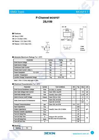
SMD Type MOSFETP-Channel MOSFET2SJ1991.70 0.1 Features VDS (V) =-100V ID =-1 A (VGS =-10V)0.42 0.10.46 0.1 RDS(ON) 2 (VGS =-10V) RDS(ON) 2.5 (VGS =-4V)1.Gate2.Drain3.Source Absolute Maximum Ratings Ta = 25Parameter Symbol Rating Unit Drain-Source Voltage VDS -100V Gate-Source Voltage VGS 20 Continuous Drain Current ID -1A Pulsed Drain Current (Note.1) IDM -2 Power Dissipation Tc = 25 PD 2 W Junction Temperature TJ 150 Junction Storage Temperature Range Tstg -55 to 150Note.1: PW 10 ms, duty cycle 50% Electrical Characteristics Ta = 25Parameter Symbol Test Conditions Min Typ Max Unit Drain-Source Breakdown Voltage VDSS ID=-250A, VGS=0V -100 V Zero Gate Voltage Drain Current IDSS VDS=-100V, VGS=0V -10 uA Gate-Body leakage current IGSS VDS=0V, VGS=20V 10 uA Gate
Keywords - ALL TRANSISTORS DATASHEET
2sj199.pdf Design, MOSFET, Power
2sj199.pdf RoHS Compliant, Service, Triacs, Semiconductor
2sj199.pdf Database, Innovation, IC, Electricity


LIST
Last Update
BJT: GA1A4M | SBT42 | 2SA200-Y | 2SA200-O | 2SD882-Q | 2SD882-P | 2SD882-E | 2SC945-L | 2SC945-H | 2SC4226-R23 | 2SC3357-F | 2SC3357-E | 2SC3356-R26 | 2SC3356-R24 | 2SC3356-R23 | 2SB772-Q | 2SB772-P | 2SB772-E | 2SA1015-L | 2SA1015-H | HSS8550
Popular searches
irfz44n | irf3205 | irfz44n datasheet | 2n4401 | bc547 transistor | bd139 | 2n4401 datasheet