View buk7528-55 datasheet:
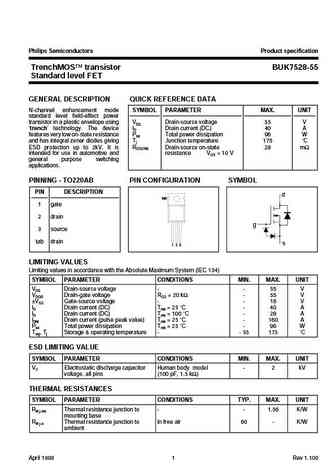
Philips Semiconductors Product specification TrenchMOS transistor BUK7528-55 Standard level FETGENERAL DESCRIPTION QUICK REFERENCE DATAN-channel enhancement mode SYMBOL PARAMETER MAX. UNITstandard level field-effect powertransistor in a plastic envelope using VDS Drain-source voltage 55 Vtrench technology. The device ID Drain current (DC) 40 Afeatures very low on-state resistance Ptot Total power dissipation 96 Wand has integral zener diodes giving Tj Junction temperature 175 CESD protection up to 2kV. It is RDS(ON) Drain-source on-state 28 mintended for use in automotive and resistance VGS = 10 Vgeneral purpose switchingapplications.PINNING - TO220AB PIN CONFIGURATION SYMBOLPIN DESCRIPTIONdtab1 gate2 draing3 sourcetab drains1 2 3LIMITING VALUESLimiting values in accordance with the Absolute Maximum System (IEC 134)SY
Keywords - ALL TRANSISTORS DATASHEET
buk7528-55.pdf Design, MOSFET, Power
buk7528-55.pdf RoHS Compliant, Service, Triacs, Semiconductor
buk7528-55.pdf Database, Innovation, IC, Electricity


LIST
Last Update
BJT: GA1A4M | SBT42 | 2SA200-Y | 2SA200-O | 2SD882-Q | 2SD882-P | 2SD882-E | 2SC945-L | 2SC945-H | 2SC4226-R23 | 2SC3357-F | 2SC3357-E | 2SC3356-R26 | 2SC3356-R24 | 2SC3356-R23 | 2SB772-Q | 2SB772-P | 2SB772-E | 2SA1015-L | 2SA1015-H | HSS8550
Popular searches
irfz44n | irf3205 | irfz44n datasheet | 2n4401 | bc547 transistor | bd139 | 2n4401 datasheet