View cep12p10 ceb12p10 datasheet:
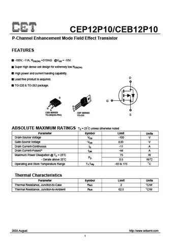
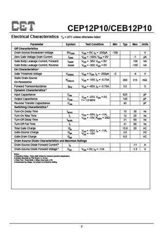
CEP12P10/CEB12P10P-Channel Enhancement Mode Field Effect TransistorFEATURES-100V, -11A, RDS(ON) =315m @VGS = -10V.Super high dense cell design for extremely low RDS(ON).High power and current handing capability.DLead free product is acquired.TO-220 & TO-263 package.GCEB SERIESCEP SERIESTO-263(DD-PAK) STO-220ABSOLUTE MAXIMUM RATINGS Tc = 25 C unless otherwise notedParameter Symbol Limit UnitsDrain-Source Voltage VDS -100 VGate-Source Voltage VGS 30 VDrain Current-Continuous ID -11 ADrain Current-Pulsed a IDM -44 AMaximum Power Dissipation @ TC = 25 C 75 WPD- Derate above 25 C 0.5 W/ COperating and Store Temperature Range TJ,Tstg -55 to 175 CThermal CharacteristicsParameter Symbol Limit UnitsThermal Resistance, Junction-to-Case RJC 2 C/WThermal Resistance, Junction-to-Ambient RJA 62.5 C/W2005.August http://www.cetsemi.com
Keywords - ALL TRANSISTORS DATASHEET
cep12p10 ceb12p10.pdf Design, MOSFET, Power
cep12p10 ceb12p10.pdf RoHS Compliant, Service, Triacs, Semiconductor
cep12p10 ceb12p10.pdf Database, Innovation, IC, Electricity


LIST
Last Update
BJT: GA1A4M | SBT42 | 2SA200-Y | 2SA200-O | 2SD882-Q | 2SD882-P | 2SD882-E | 2SC945-L | 2SC945-H | 2SC4226-R23 | 2SC3357-F | 2SC3357-E | 2SC3356-R26 | 2SC3356-R24 | 2SC3356-R23 | 2SB772-Q | 2SB772-P | 2SB772-E | 2SA1015-L | 2SA1015-H | HSS8550
Popular searches
irfz44n | irf3205 | irfz44n datasheet | 2n4401 | bc547 transistor | bd139 | 2n4401 datasheet