View irf5210 datasheet:
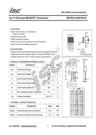
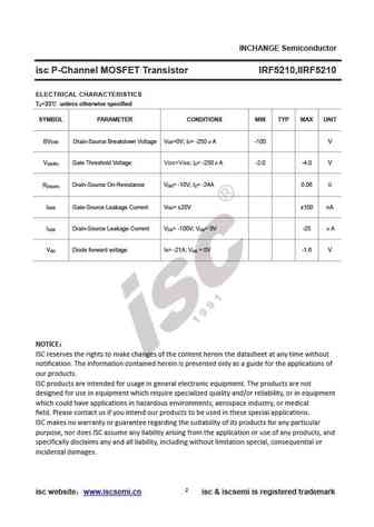
INCHANGE Semiconductorisc P-Channel MOSFET Transistor IRF5210,IIRF5210FEATURESStatic drain-source on-resistance:RDS(on)0.06Enhancement mode:100% avalanche testedMinimum Lot-to-Lot variations for robust deviceperformance and reliable operationDESCRIPTIONCombine with the fast switching speed and ruggedized devicedesign,provide the designer with an extremely efficient andreliable device for use in a wide variety of applications.ABSOLUTE MAXIMUM RATINGS(T =25)aSYMBOL PARAMETER VALUE UNITV Drain-Source Voltage -100 VDSSV Gate-Source Voltage 20 VGSI Drain Current-Continuous -40 ADI Drain Current-Single Pulsed -140 ADMP Total Dissipation @T =25 200 WD CMax. Operating Junction Temperature 175 TjT Storage Temperature -55~175 stgTHERMAL CHARACTERISTICSSYMBOL PARAMETER MAX UNIT/WRth(j-c)
Keywords - ALL TRANSISTORS DATASHEET
irf5210.pdf Design, MOSFET, Power
irf5210.pdf RoHS Compliant, Service, Triacs, Semiconductor
irf5210.pdf Database, Innovation, IC, Electricity


LIST
Last Update
BJT: GA1A4M | SBT42 | 2SA200-Y | 2SA200-O | 2SD882-Q | 2SD882-P | 2SD882-E | 2SC945-L | 2SC945-H | 2SC4226-R23 | 2SC3357-F | 2SC3357-E | 2SC3356-R26 | 2SC3356-R24 | 2SC3356-R23 | 2SB772-Q | 2SB772-P | 2SB772-E | 2SA1015-L | 2SA1015-H | HSS8550
Popular searches
irfz44n | irf3205 | irfz44n datasheet | 2n4401 | bc547 transistor | bd139 | 2n4401 datasheet