View ntd12n10 datasheet:
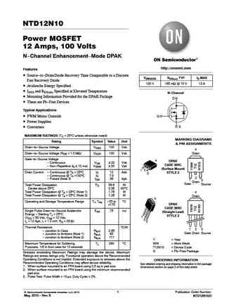
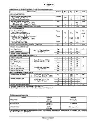
NTD12N10Power MOSFET12 Amps, 100 VoltsN-Channel Enhancement-Mode DPAKhttp://onsemi.comFeatures Source-to-Drain Diode Recovery Time Comparable to a DiscreteV(BR)DSS RDS(on) TYP ID MAXFast Recovery Diode100 V 165 mW @ 10 V 12 A Avalanche Energy Specified IDSS and RDS(on) Specified at Elevated TemperatureN-Channel Mounting Information Provided for the DPAK PackageD These are Pb-Free DevicesTypical Applications PWM Motor Controls G Power SuppliesS ConvertersMAXIMUM RATINGS (TC = 25C unless otherwise noted)MARKING DIAGRAMSRating Symbol Value Unit& PIN ASSIGNMENTSDrain-to-Source Voltage VDSS 100 Vdc4Drain-to-Source Voltage (RGS = 1.0 MW) VDGR 100 Vdc DrainGate-to-Source Voltage4DPAK- Continuous VGS 20 VdcCASE 369C- Non-Repetitive (tp 10 ms) VGSM 30 Vpk(Surface Mount)21Drain Current
Keywords - ALL TRANSISTORS DATASHEET
ntd12n10.pdf Design, MOSFET, Power
ntd12n10.pdf RoHS Compliant, Service, Triacs, Semiconductor
ntd12n10.pdf Database, Innovation, IC, Electricity


LIST
Last Update
BJT: GA1A4M | SBT42 | 2SA200-Y | 2SA200-O | 2SD882-Q | 2SD882-P | 2SD882-E | 2SC945-L | 2SC945-H | 2SC4226-R23 | 2SC3357-F | 2SC3357-E | 2SC3356-R26 | 2SC3356-R24 | 2SC3356-R23 | 2SB772-Q | 2SB772-P | 2SB772-E | 2SA1015-L | 2SA1015-H | HSS8550
Popular searches
irfz44n | irf3205 | irfz44n datasheet | 2n4401 | bc547 transistor | bd139 | 2n4401 datasheet