View ntgd4167c datasheet:
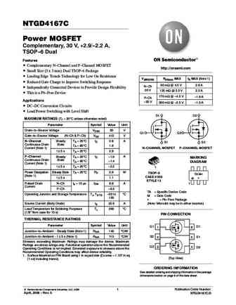
NTGD4167CPower MOSFETComplementary, 30 V, +2.9/-2.2 A,TSOP-6 DualFeatures Complementary N-Channel and P-Channel MOSFEThttp://onsemi.com Small Size (3 x 3 mm) Dual TSOP-6 Package Leading Edge Trench Technology for Low On ResistanceV(BR)DSS RDS(on) MAX ID MAX (Note 1) Reduced Gate Charge to Improve Switching Response90 mW @ 4.5 V 2.6 AN-Ch Independently Connected Devices to Provide Design Flexibility20 V125 mW @ 2.5 V 2.2 A This is a Pb-Free Device170 mW @ -4.5 V -1.9 AP-ChApplications-20 V300 mW @ -2.5 V -1.0 A DC-DC Conversion Circuits Load/Power Switching with Level ShiftD1 D2MAXIMUM RATINGS (TJ = 25C unless otherwise noted)Parameter Symbol Value UnitDrain-to-Source Voltage VDSS 30 VG1 G2Gate-to-Source Voltage (N-Ch & P-Ch) VGS 12 VN-Channel Steady TA = 25C ID 2.6 AS1 S2Continuous Drain Stat
Keywords - ALL TRANSISTORS DATASHEET
ntgd4167c.pdf Design, MOSFET, Power
ntgd4167c.pdf RoHS Compliant, Service, Triacs, Semiconductor
ntgd4167c.pdf Database, Innovation, IC, Electricity


LIST
Last Update
BJT: GA1A4M | SBT42 | 2SA200-Y | 2SA200-O | 2SD882-Q | 2SD882-P | 2SD882-E | 2SC945-L | 2SC945-H | 2SC4226-R23 | 2SC3357-F | 2SC3357-E | 2SC3356-R26 | 2SC3356-R24 | 2SC3356-R23 | 2SB772-Q | 2SB772-P | 2SB772-E | 2SA1015-L | 2SA1015-H | HSS8550
Popular searches
irfz44n | irf3205 | irfz44n datasheet | 2n4401 | bc547 transistor | bd139 | 2n4401 datasheet