View ptw40n50 datasheet:
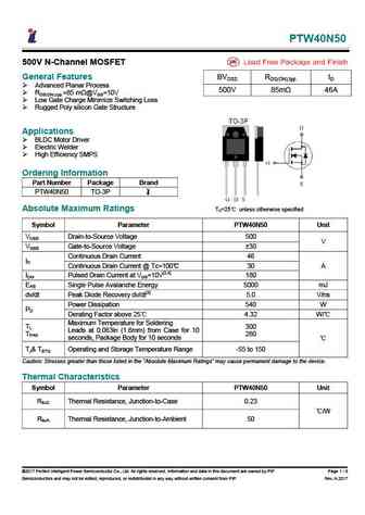
PTW40N50 500V N-Channel MOSFET General Features BVDSS RDS(ON),typ. ID Advanced Planar Process 500V 85m 46A RDS(ON),typ.=85 m@VGS=10V Low Gate Charge Minimize Switching Loss Rugged Poly silicon Gate Structure Applications BLDC Motor Driver Electric Welder High Efficiency SMPS Ordering Information Part Number Package Brand PTW40N50 TO-3P Absolute Maximum Ratings T =25 unless otherwise specified CSymbol Parameter PTW40N50 Unit VDSS Drain-to-Source Voltage 500 V VGSS Gate-to-Source Voltage 30 Continuous Drain Current 46 ID Continuous Drain Current @ Tc=100 30 A IDM Pulsed Drain Current at VGS=10V[2,4] 180 EAS Single Pulse Avalanche Energy 5000 mJ dv/dt Peak Diode Recovery dv/dt[3] 5.0 V/ns Power Dissipation 540 W PD Derating Factor above 25 4.32 W/ Maximum Temperature for Soldering
Keywords - ALL TRANSISTORS DATASHEET
ptw40n50.pdf Design, MOSFET, Power
ptw40n50.pdf RoHS Compliant, Service, Triacs, Semiconductor
ptw40n50.pdf Database, Innovation, IC, Electricity


LIST
Last Update
BJT: GA1A4M | SBT42 | 2SA200-Y | 2SA200-O | 2SD882-Q | 2SD882-P | 2SD882-E | 2SC945-L | 2SC945-H | 2SC4226-R23 | 2SC3357-F | 2SC3357-E | 2SC3356-R26 | 2SC3356-R24 | 2SC3356-R23 | 2SB772-Q | 2SB772-P | 2SB772-E | 2SA1015-L | 2SA1015-H | HSS8550
Popular searches
irfz44n | irf3205 | irfz44n datasheet | 2n4401 | bc547 transistor | bd139 | 2n4401 datasheet