2N5632 Datasheet, Equivalent, Cross Reference Search
Type Designator: 2N5632
Material of Transistor: Si
Polarity: NPN
Maximum Collector Power Dissipation (Pc): 150 W
Maximum Collector-Base Voltage |Vcb|: 100 V
Maximum Collector-Emitter Voltage |Vce|: 100 V
Maximum Emitter-Base Voltage |Veb|: 7 V
Maximum Collector Current |Ic max|: 15 A
Max. Operating Junction Temperature (Tj): 200 °C
Transition Frequency (ft): 1 MHz
Collector Capacitance (Cc): 300 pF
Forward Current Transfer Ratio (hFE), MIN: 25
Noise Figure, dB: -
Package: TO3
2N5632 Transistor Equivalent Substitute - Cross-Reference Search
2N5632 Datasheet (PDF)
2n5632.pdf

2N5632Dimensions in mm (inches). Bipolar NPN Device in a Hermetically sealed TO3 25.15 (0.99)6.35 (0.25) 26.67 (1.05)9.15 (0.36)Metal Package. 10.67 (0.42)11.18 (0.44) 1.52 (0.06)3.43 (0.135)1 2 Bipolar NPN Device. 3VCEO = 100V (case)3.84 (0.151)4.09 (0.161)7.92 (0.312) IC = 10A 12.70 (0.50) All Semelab hermetically sealed products can be processed in
2n5632 2n5633 2n5634.pdf


Product Specification www.jmnic.com Silicon NPN Power Transistors 2N5632 2N5633 2N5634 DESCRIPTION With TO-3 package Low collector-emitter saturation voltage APPLICATIONS For general-purpose power amplifier and switching applications PINNING PIN DESCRIPTION1 Base 2 Emitter3 CollectorFig.1 simplified outline (TO-3) and symbolAbsolute maximum ratings(Ta=) SY
2n5632 2n5633 2n5634.pdf
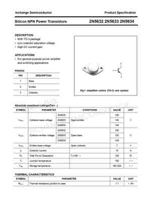

Inchange Semiconductor Product Specification Silicon NPN Power Transistors 2N5632 2N5633 2N5634 DESCRIPTION With TO-3 package Low collector saturation voltage High DC current gain APPLICATIONS For general-purpose power amplifier and switching applications PINNING PIN DESCRIPTION1 Base 2 EmitterFig.1 simplified outline (TO-3) and symbol 3 CollectorAbsolute m
2n5630 2n6030 2n5631 2n6031.pdf


Order this documentMOTOROLAby 2N5630/DSEMICONDUCTOR TECHNICAL DATANPN2N5630High-Voltage High Power2N5631TransistorsPNP. . . designed for use in high power audio amplifier applicat
2n5639.pdf


2N5639N-Channel Switch This device is designed for low level analog switchng, sample and hold circuits and chopper stabilized amplifiers. Sourced from process 51.TO-9211. Drain 2. Source 3. GateAbsolute Maximum Ratings * TC=25C unless otherwise notedSymbol Parameter Value UnitsVDG Drain-Gate Voltage 30 VVGS Gate-Source Voltage -30 VIGF Forward Gate Current 50 mA
2n5638.pdf


2N5638N-Channel Switch This device is designed for low level analog switchng, sample and hold circuits and chopper stabilized amplifiers. Sourced from process 51.TO-9211. Drain 2. Source 3. GateAbsolute Maximum Ratings * TC=25C unless otherwise notedSymbol Parameter Value UnitsVDG Drain-Gate Voltage 30 VVGS Gate-Source Voltage -30 VIGF Forward Gate Current 50 mA
2n5629 2n5630 2n6029 2n6030.pdf

145 Adams Avenue, Hauppauge, NY 11788 USATel: (631) 435-1110 Fax: (631) 435-1824
2n5638 2n5639.pdf


2N5638, 2N56392N5638 is a Preferred DeviceJFET Chopper TransistorsN-Channel - DepletionN-Channel Junction Field Effect Transistors, depletion mode(Type A) designed for chopper and high-speed switching applications.Featureshttp://onsemi.com Low Drain-Source ON Resistance: RDS(on) = 30W for 2N5638RDS(on) = 60W for 2N56391 DRAIN Low Reverse Transfer Capacitance -
2n5631-d.pdf

2N5631High-Voltage - High PowerTransistorsHigh-voltage - high power transistors designed for use in highpower audio amplifier applications and high voltage switchingregulator circuits.http://onsemi.com High Collector Emitter Sustaining Voltage -VCEO(sus) = 140 Vdc16 AMPERE High DC Current Gain - @ IC = 8.0 AdchFE = 15 (Min)POWER TRANSISTORS Low Collector-Emitt
2n5633.pdf

2N5633Dimensions in mm (inches). Bipolar NPN Device in a Hermetically sealed TO3 25.15 (0.99)6.35 (0.25) 26.67 (1.05)9.15 (0.36)Metal Package. 10.67 (0.42)11.18 (0.44) 1.52 (0.06)3.43 (0.135)1 2 Bipolar NPN Device. 3VCEO = 80V (case)3.84 (0.151)4.09 (0.161)7.92 (0.312) IC = 10A 12.70 (0.50) All Semelab hermetically sealed products can be processed in a
2n5634.pdf

2N5634Dimensions in mm (inches). Bipolar NPN Device in a Hermetically sealed TO3 25.15 (0.99)6.35 (0.25) 26.67 (1.05)9.15 (0.36)Metal Package. 10.67 (0.42)11.18 (0.44) 1.52 (0.06)3.43 (0.135)1 2 Bipolar NPN Device. 3VCEO = 140V (case)3.84 (0.151)4.09 (0.161)7.92 (0.312) IC = 10A 12.70 (0.50) All Semelab hermetically sealed products can be processed in
2n5629 2n5630.pdf


Product Specification www.jmnic.com Silicon NPN Power Transistors 2N5629 2N5630 DESCRIPTION With TO-3 package Complement to type 2N6029 2N6030 APPLICATIONS For high voltage and high power amplifier applications PINNING PIN DESCRIPTION1 Base 2 Emitter3 CollectorFig.1 simplified outline (TO-3) and symbolAbsolute maximum ratings(Ta=) SYMBOL PARAMETER CONDITIO
2n5631.pdf


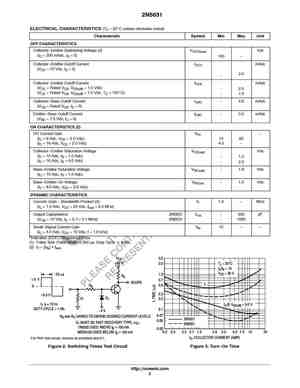
Product Specification www.jmnic.com Silicon NPN Power Transistors 2N5631 DESCRIPTION With TO-3 package Complement to type 2N6031 High collector-emitter sustaining voltage High DC current gain Low collector-emitter saturation voltage APPLICATIONS For high power audio amplifier and high voltage switching regulator circuits applications PINNING PIN DESCRIPTION
2n5631.pdf


SPTECH Product SpecificationSPTECH Silicon NPN Power Transistor 2N5631DESCRIPTIONExcellent Safe Operating AreaHigh DC Current Gain-h = 15(Min)@I = 8AFE CLow Saturation Voltage-: V )= 1.0V(Max)@ I = 10ACE(sat CComplement to Type 2N6031APPLICATIONSDesigned for use in high power audio amplifier applicationsand high voltage switching regulator circuits.ABSOLUTE M
2n5629 2n5630.pdf
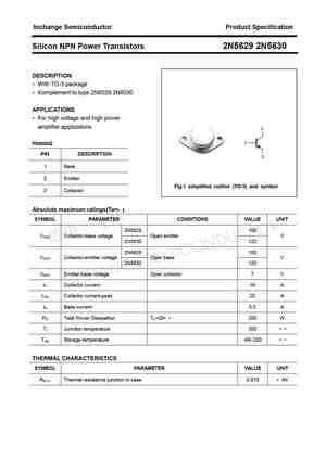

Inchange Semiconductor Product Specification Silicon NPN Power Transistors 2N5629 2N5630 DESCRIPTION With TO-3 package Complement to type 2N6029 2N6030 APPLICATIONS For high voltage and high power amplifier applications PINNING PIN DESCRIPTION1 Base 2 EmitterFig.1 simplified outline (TO-3) and symbol 3 CollectorAbsolute maximum ratings(Ta=) SYMBOL PARAMETE
2n5631.pdf


Inchange Semiconductor Product Specification Silicon NPN Power Transistors 2N5631 DESCRIPTION With TO-3 package Complement to type 2N6031 High collector-emitter sustaining voltage High DC current gain@IC=8A Low collector saturation voltage APPLICATIONS For high power audio amplifier and high voltage switching regulator circuits applications PINNING PIN DESC
Datasheet: 2N3200 , 2N3201 , 2N3202 , 2N3203 , 2N3204 , 2N3205 , 2N3206 , 2N3207 , 2SC945 , 2N3209 , 2N3209AQF , 2N3209CSM , 2N3209DCSM , 2N3209L , 2N321 , 2N3210 , 2N3211 .


