2N5632. Аналоги и основные параметры
Наименование производителя: 2N5632
Тип материала: Si
Полярность: NPN
Предельные значения
Максимальная рассеиваемая мощность (Pc): 150 W
Макcимально допустимое напряжение коллектор-база (Ucb): 100 V
Макcимально допустимое напряжение коллектор-эмиттер (Uce): 100 V
Макcимально допустимое напряжение эмиттер-база (Ueb): 7 V
Макcимальный постоянный ток коллектора (Ic): 15 A
Предельная температура PN-перехода (Tj): 200 °C
Электрические характеристики
Граничная частота коэффициента передачи тока (ft): 1 MHz
Ёмкость коллекторного перехода (Cc): 300 pf
Статический коэффициент передачи тока (hFE): 25
Корпус транзистора: TO3
Аналоги (замена) для 2N5632
- подборⓘ биполярного транзистора по параметрам
2N5632 даташит
..1. Size:11K semelab
2n5632.pdf 
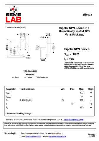
2N5632 Dimensions in mm (inches). Bipolar NPN Device in a Hermetically sealed TO3 25.15 (0.99) 6.35 (0.25) 26.67 (1.05) 9.15 (0.36) Metal Package. 10.67 (0.42) 11.18 (0.44) 1.52 (0.06) 3.43 (0.135) 1 2 Bipolar NPN Device. 3 VCEO = 100V (case) 3.84 (0.151) 4.09 (0.161) 7.92 (0.312) IC = 10A 12.70 (0.50) All Semelab hermetically sealed products can be processed in
..2. Size:103K jmnic
2n5632 2n5633 2n5634.pdf 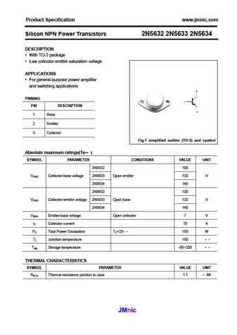
Product Specification www.jmnic.com Silicon NPN Power Transistors 2N5632 2N5633 2N5634 DESCRIPTION With TO-3 package Low collector-emitter saturation voltage APPLICATIONS For general-purpose power amplifier and switching applications PINNING PIN DESCRIPTION 1 Base 2 Emitter 3 Collector Fig.1 simplified outline (TO-3) and symbol Absolute maximum ratings(Ta= ) SY
..3. Size:117K inchange semiconductor
2n5632 2n5633 2n5634.pdf 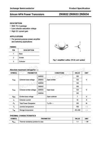
Inchange Semiconductor Product Specification Silicon NPN Power Transistors 2N5632 2N5633 2N5634 DESCRIPTION With TO-3 package Low collector saturation voltage High DC current gain APPLICATIONS For general-purpose power amplifier and switching applications PINNING PIN DESCRIPTION 1 Base 2 Emitter Fig.1 simplified outline (TO-3) and symbol 3 Collector Absolute m
9.1. Size:253K motorola
2n5630 2n6030 2n5631 2n6031.pdf 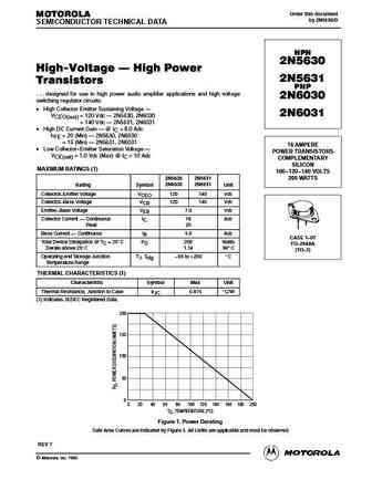
Order this document MOTOROLA by 2N5630/D SEMICONDUCTOR TECHNICAL DATA NPN 2N5630 High-Voltage High Power 2N5631 Transistors PNP . . . designed for use in high power audio amplifier applications and high voltage 2N6030 switching regulator circuits. High Collector Emitter Sustaining Voltage 2N6031 VCEO(sus) = 120 Vdc 2N5630, 2N6030 VCEO(sus) = 140 Vdc 2N5631, 2N603
9.2. Size:26K fairchild semi
2n5639.pdf 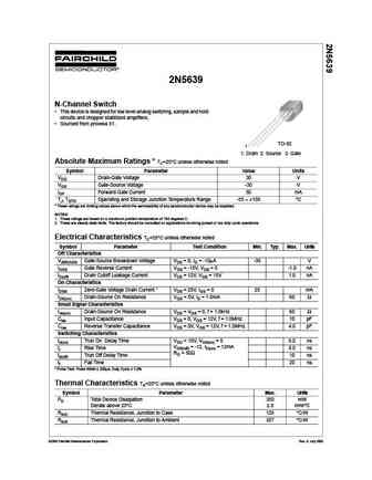
2N5639 N-Channel Switch This device is designed for low level analog switchng, sample and hold circuits and chopper stabilized amplifiers. Sourced from process 51. TO-92 1 1. Drain 2. Source 3. Gate Absolute Maximum Ratings * TC=25 C unless otherwise noted Symbol Parameter Value Units VDG Drain-Gate Voltage 30 V VGS Gate-Source Voltage -30 V IGF Forward Gate Current 50 mA
9.3. Size:26K fairchild semi
2n5638.pdf 
2N5638 N-Channel Switch This device is designed for low level analog switchng, sample and hold circuits and chopper stabilized amplifiers. Sourced from process 51. TO-92 1 1. Drain 2. Source 3. Gate Absolute Maximum Ratings * TC=25 C unless otherwise noted Symbol Parameter Value Units VDG Drain-Gate Voltage 30 V VGS Gate-Source Voltage -30 V IGF Forward Gate Current 50 mA
9.5. Size:51K onsemi
2n5638 2n5639.pdf 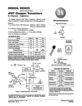
2N5638, 2N5639 2N5638 is a Preferred Device JFET Chopper Transistors N-Channel - Depletion N-Channel Junction Field Effect Transistors, depletion mode (Type A) designed for chopper and high-speed switching applications. Features http //onsemi.com Low Drain-Source ON Resistance RDS(on) = 30W for 2N5638 RDS(on) = 60W for 2N5639 1 DRAIN Low Reverse Transfer Capacitance -
9.6. Size:198K onsemi
2n5631-d.pdf 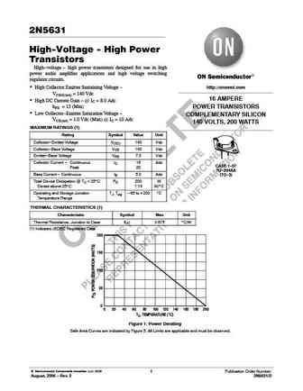
2N5631 High-Voltage - High Power Transistors High-voltage - high power transistors designed for use in high power audio amplifier applications and high voltage switching regulator circuits. http //onsemi.com High Collector Emitter Sustaining Voltage - VCEO(sus) = 140 Vdc 16 AMPERE High DC Current Gain - @ IC = 8.0 Adc hFE = 15 (Min) POWER TRANSISTORS Low Collector-Emitt
9.7. Size:11K semelab
2n5633.pdf 
2N5633 Dimensions in mm (inches). Bipolar NPN Device in a Hermetically sealed TO3 25.15 (0.99) 6.35 (0.25) 26.67 (1.05) 9.15 (0.36) Metal Package. 10.67 (0.42) 11.18 (0.44) 1.52 (0.06) 3.43 (0.135) 1 2 Bipolar NPN Device. 3 VCEO = 80V (case) 3.84 (0.151) 4.09 (0.161) 7.92 (0.312) IC = 10A 12.70 (0.50) All Semelab hermetically sealed products can be processed in a
9.8. Size:11K semelab
2n5634.pdf 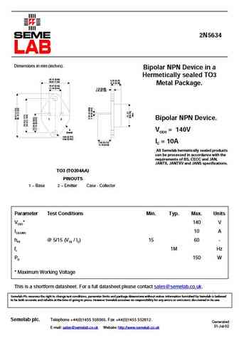
2N5634 Dimensions in mm (inches). Bipolar NPN Device in a Hermetically sealed TO3 25.15 (0.99) 6.35 (0.25) 26.67 (1.05) 9.15 (0.36) Metal Package. 10.67 (0.42) 11.18 (0.44) 1.52 (0.06) 3.43 (0.135) 1 2 Bipolar NPN Device. 3 VCEO = 140V (case) 3.84 (0.151) 4.09 (0.161) 7.92 (0.312) IC = 10A 12.70 (0.50) All Semelab hermetically sealed products can be processed in
9.9. Size:118K jmnic
2n5629 2n5630.pdf 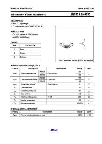
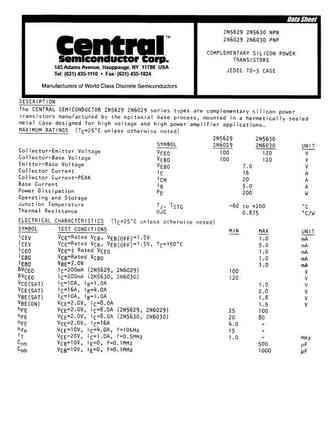
Product Specification www.jmnic.com Silicon NPN Power Transistors 2N5629 2N5630 DESCRIPTION With TO-3 package Complement to type 2N6029 2N6030 APPLICATIONS For high voltage and high power amplifier applications PINNING PIN DESCRIPTION 1 Base 2 Emitter 3 Collector Fig.1 simplified outline (TO-3) and symbol Absolute maximum ratings(Ta= ) SYMBOL PARAMETER CONDITIO
9.10. Size:99K jmnic
2n5631.pdf 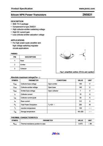
Product Specification www.jmnic.com Silicon NPN Power Transistors 2N5631 DESCRIPTION With TO-3 package Complement to type 2N6031 High collector-emitter sustaining voltage High DC current gain Low collector-emitter saturation voltage APPLICATIONS For high power audio amplifier and high voltage switching regulator circuits applications PINNING PIN DESCRIPTION
9.11. Size:167K cn sptech
2n5631.pdf 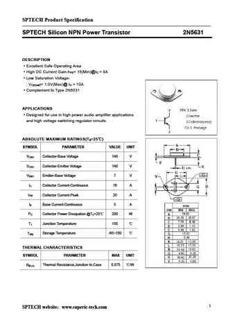
SPTECH Product Specification SPTECH Silicon NPN Power Transistor 2N5631 DESCRIPTION Excellent Safe Operating Area High DC Current Gain-h = 15(Min)@I = 8A FE C Low Saturation Voltage- V )= 1.0V(Max)@ I = 10A CE(sat C Complement to Type 2N6031 APPLICATIONS Designed for use in high power audio amplifier applications and high voltage switching regulator circuits. ABSOLUTE M
9.12. Size:118K inchange semiconductor
2n5629 2n5630.pdf 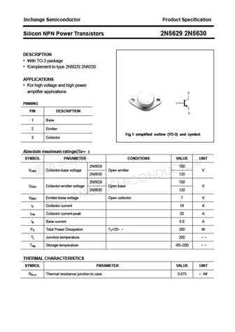
Inchange Semiconductor Product Specification Silicon NPN Power Transistors 2N5629 2N5630 DESCRIPTION With TO-3 package Complement to type 2N6029 2N6030 APPLICATIONS For high voltage and high power amplifier applications PINNING PIN DESCRIPTION 1 Base 2 Emitter Fig.1 simplified outline (TO-3) and symbol 3 Collector Absolute maximum ratings(Ta= ) SYMBOL PARAMETE
9.13. Size:117K inchange semiconductor
2n5631.pdf 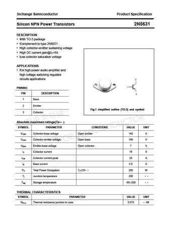
Inchange Semiconductor Product Specification Silicon NPN Power Transistors 2N5631 DESCRIPTION With TO-3 package Complement to type 2N6031 High collector-emitter sustaining voltage High DC current gain@IC=8A Low collector saturation voltage APPLICATIONS For high power audio amplifier and high voltage switching regulator circuits applications PINNING PIN DESC
Другие транзисторы: 2N5625, 2N5626, 2N5627, 2N5628, 2N5629, 2N563, 2N5630, 2N5631, MJE340, 2N5633, 2N5634, 2N5635, 2N5636, 2N5637, 2N564, 2N5641, 2N5642