2N6570 Datasheet, Equivalent, Cross Reference Search
Type Designator: 2N6570
Material of Transistor: Si
Polarity: NPN
Maximum Collector Power Dissipation (Pc): 250 W
Maximum Collector-Base Voltage |Vcb|: 100 V
Maximum Collector-Emitter Voltage |Vce|: 90 V
Maximum Emitter-Base Voltage |Veb|: 7 V
Maximum Collector Current |Ic max|: 40 A
Max. Operating Junction Temperature (Tj): 200 °C
Transition Frequency (ft): 1 MHz
Forward Current Transfer Ratio (hFE), MIN: 20
Noise Figure, dB: -
Package: TO3
2N6570 Transistor Equivalent Substitute - Cross-Reference Search
2N6570 Datasheet (PDF)
2n6576 2n6577 2n6578.pdf

Order this documentMOTOROLAby 2N6576/DSEMICONDUCTOR TECHNICAL DATA2N65762N6577NPN Silicon Power Darlington2N6578TransistorsGeneral purpose EpiBase power Darlington transistors, suit
2n6576 2n6577 2n6578.pdf


145 Adams Avenue, Hauppauge, NY 11788 USATel: (631) 435-1110 Fax: (631) 435-1824
2n6575.pdf

2N6575Dimensions in mm (inches). Bipolar NPN Device in a Hermetically sealed TO3 25.15 (0.99)6.35 (0.25) 26.67 (1.05)9.15 (0.36)Metal Package. 10.67 (0.42)11.18 (0.44) 1.52 (0.06)3.43 (0.135)1 2 Bipolar NPN Device. 3VCEO = 300V (case)3.84 (0.151)4.09 (0.161)7.92 (0.312) IC = 10A 12.70 (0.50) All Semelab hermetically sealed products can be processed in
2n657.pdf
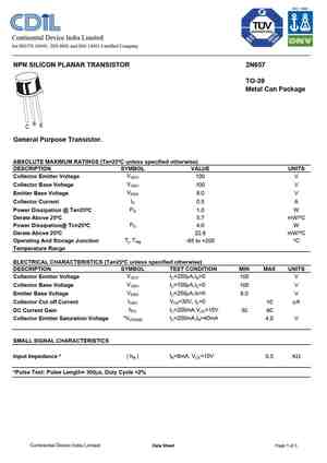

Continental Device India LimitedAn ISO/TS 16949, ISO 9001 and ISO 14001 Certified CompanyNPN SILICON PLANAR TRANSISTOR 2N657TO-39Metal Can PackageGeneral Purpose Transistor.ABSOLUTE MAXIMUM RATINGS (Ta=25C unless specified otherwise)DESCRIPTION SYMBOL VALUE UNITSVCEOCollector Emitter Voltage 100 VVCBOCollector Base Voltage 100 VVEBOEmitter Base Voltage 8.0 VICCol
2n6576 2n7577 2n7578.pdf

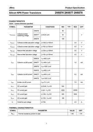
JMnic Product Specification Silicon NPN Power Transistors 2N6576 2N6577 2N6578 DESCRIPTION With TO-3 package DARLINGTON High DC current gain APPLICATIONS Power switching Audio amplifiers Hammer drivers Series and shunt regulators PINNING PIN DESCRIPTION1 Base 2 EmitterFig.1 simplified outline (TO-3) and symbol 3 CollectorAbsolute maximum ratings(T
2n6576 2n6577 2n6578.pdf


Inchange Semiconductor Product Specification Silicon NPN Power Transistors 2N6576 2N6577 2N6578 DESCRIPTION With TO-3 package DARLINGTON High DC current gain APPLICATIONS Power switching Audio amplifiers Hammer drivers Series and shunt regulators PINNING PIN DESCRIPTION1 Base 2 EmitterFig.1 simplified outline (TO-3) and symbol 3 CollectorAbsolute
2n6575.pdf


isc Silicon NPN Power Transistor 2N6575DESCRIPTIONCollector-Emitter Sustaining Voltage-: V = 300V(Min.)CEOFast Switching SpeedHigh Current Capability100% avalanche testedMinimum Lot-to-Lot variations for robust deviceperformance and reliable operationAPPLICATIONSDesigned for converters, inverters, pulse-width- modulatedregulators and a variety of power switch
2n6574.pdf


isc Silicon NPN Power Transistor 2N6574DESCRIPTIONCollector-Emitter Sustaining Voltage-: V = 275V(Min.)CEOFast Switching SpeedHigh Current Capability100% avalanche testedMinimum Lot-to-Lot variations for robust deviceperformance and reliable operationAPPLICATIONSDesigned for converters, inverters, pulse-width- modulatedregulators and a variety of power switch
2n6573.pdf


isc Silicon NPN Power Transistor 2N6573DESCRIPTIONCollector-Emitter Sustaining Voltage-: V = 250V(Min.)CEOFast Switching SpeedHigh Current Capability100% avalanche testedMinimum Lot-to-Lot variations for robust deviceperformance and reliable operationAPPLICATIONSDesigned for converters, inverters, pulse-width- modulatedregulators and a variety of power switch
2n6579.pdf


INCHANGE Semiconductorisc Silicon NPN Power Transistor 2N6579DESCRIPTIONExcellent Safe Operating AreaHigh Voltage,High SpeedLow Saturation VoltageCollector-Emitter Sustaining Voltage-: V = 350V(Min)CEO(SUS)Minimum Lot-to-Lot variations for robust deviceperformance and reliable operationAPPLICATIONSOff-line power suppliesSwitching amplifiersInverters/C
Datasheet: 2N3200 , 2N3201 , 2N3202 , 2N3203 , 2N3204 , 2N3205 , 2N3206 , 2N3207 , 2SC945 , 2N3209 , 2N3209AQF , 2N3209CSM , 2N3209DCSM , 2N3209L , 2N321 , 2N3210 , 2N3211 .


