View bmdfn2301 detailed specification:
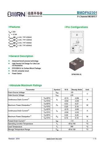
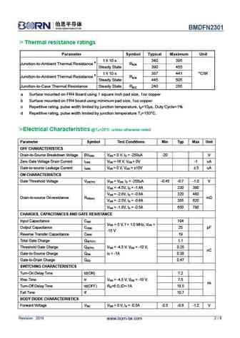
BMDFN2301 P-Channel MOSFET Features Pin Configurations V = -20V DS I D = -0.74A D R @V = -4.5V, TYP =230m DS(ON) GS R @V = -2.8V, TYP =320m DS(ON) GS R @V = -2.5V, TYP =355m DS(ON) GS R @V = -1.8V, TYP =650m DS(ON) GS S G General Description G Advanced trench process technology S D High Density Cell Design For Ultra Low On-Resistance DFN1006-3L for Surface Mount Package DC-DC converter circuit Power Switch DFN1006-3L Absolute Maximum Ratings Parameter Symbol 10 S Steady State Unit Drain-Source Voltage VDS -20 V Gate-Source Voltage VGS 10 TA=25 -0.74 -0.69 C Continuous Drain Current a ID A TA=70 -0.59 -0.55 C TA=25 0.32 0.27 C Maximum Power Dissipation a PD W TA=70 0.20 0.18 C TA=25 -0.70 -0.65 C Continuous Drain Current b ID A TA=70 -0.56 -0.52 C TA=25 0.28 0.25... See More ⇒
Keywords - ALL TRANSISTORS SPECS
bmdfn2301.pdf Design, MOSFET, Power
bmdfn2301.pdf RoHS Compliant, Service, Triacs, Semiconductor
bmdfn2301.pdf Database, Innovation, IC, Electricity
BJT Parameters and How They Relate
🌐 : EN ES РУ

LIST
Last Update
BJT: ZDT6705 | GA1L4Z | GA1A4M | SBT42 | 2SA200-Y | 2SA200-O
Popular searches
irfz44n | irf3205 | irfz44n datasheet | 2n4401 | bc547 transistor | bd139 | 2n4401 datasheet