View bmdfn2302 detailed specification:
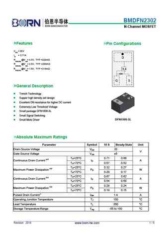
BMDFN2302 N-Channel MOSFET Features Pin Configurations V = 20V DS I D = 0.71A D R @V = 4.5V, TYP =220m DS(ON) GS R @V = 2.5V, TYP =260m DS(ON) GS R @V = 1.8V, TYP =315m DS(ON) GS G S General Description Trench Technology G S Supper high density cell design D Excellent ON resistance for higher DC current Extremely Low Threshold Voltage Small package DFN1006-3L Small Signal Switching DFN1006-3L Small Moto Driver Absolute Maximum Ratings Parameter Symbol 10 S Steady State Unit Drain-Source Voltage VDS 20 V Gate-Source Voltage VGS 5 T =25 C 0.71 0.66 A Continuous Drain Current a d I A D T =70 C 0.57 0.52 A T =25 C 0.32 0.27 A Maximum Power Dissipation a d P W D T =70 C 0.20 0.17 A T =25 C 0.67 0.62 A Continuous Drain Current b d I A D T =70 C 0.54 0.50 A T =25 C 0... See More ⇒
Keywords - ALL TRANSISTORS SPECS
bmdfn2302.pdf Design, MOSFET, Power
bmdfn2302.pdf RoHS Compliant, Service, Triacs, Semiconductor
bmdfn2302.pdf Database, Innovation, IC, Electricity
BJT Parameters and How They Relate
🌐 : EN ES РУ

LIST
Last Update
BJT: ZDT6705 | GA1L4Z | GA1A4M | SBT42 | 2SA200-Y | 2SA200-O
Popular searches
irfz44n | irf3205 | irfz44n datasheet | 2n4401 | bc547 transistor | bd139 | 2n4401 datasheet