View bms2302 detailed specification:
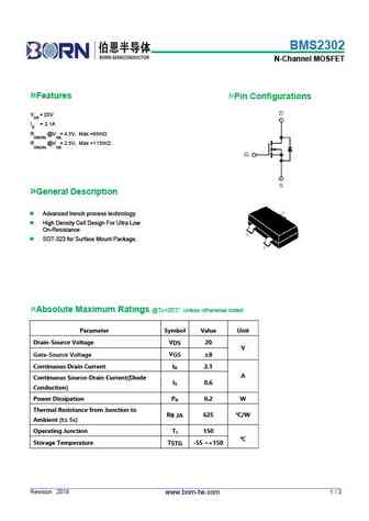
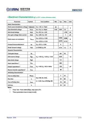
BMS2302 N-Channel MOSFET Features Pin Configurations V = 20V DS I D = 2.1A R @V = 4.5V, Max =68m DS(ON) GS R @V = 2.5V, Max =115m DS(ON) GS General Description Advanced trench process technology High Density Cell Design For Ultra Low On-Resistance SOT-323 for Surface Mount Package. Absolute Maximum Ratings @T =25 unless otherwise noted A Parameter Symbol Value Unit Drain-Source Voltage VDS 20 V Gate-Source Voltage V 8 GS Continuous Drain Current I 2.1 D A Continuous Source-Drain Current(Diode I 0.6 S Conduction) Power Dissipation PD 0.2 W Thermal Resistance from Junction to R JA 625 /W Ambient (t 5s) Operating Junction T 150 J Storage Temperature T -55 +150 STG Revision 2018 1 / 3 www.born-tw.com BMS2302 Electrical Characteristics @T =25 unless otherwise noted A ... See More ⇒
Keywords - ALL TRANSISTORS SPECS
bms2302.pdf Design, MOSFET, Power
bms2302.pdf RoHS Compliant, Service, Triacs, Semiconductor
bms2302.pdf Database, Innovation, IC, Electricity
BJT Parameters and How They Relate
🌐 : EN ES РУ

LIST
Last Update
BJT: ZDT6705 | GA1L4Z | GA1A4M | SBT42 | 2SA200-Y | 2SA200-O
Popular searches
irfz44n | irf3205 | irfz44n datasheet | 2n4401 | bc547 transistor | bd139 | 2n4401 datasheet