View cem4207 detailed specification:
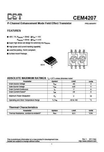
CEM4207 P-Channel Enhancement Mode Field Effect Transistor PRELIMINARY FEATURES -40V, -7A, RDS(ON) = 30m @VGS = -10V. RDS(ON) = 40m @VGS = -4.5V. Super high dense cell design for extremely low RDS(ON). High power and current handing capability. D1 D1 D2 D2 Lead-free plating ; RoHS compliant. 8 7 6 5 Surface mount Package. SO-8 1 2 3 4 1 S1 G1 S2 G2 ABSOLUTE MAXIMUM RATINGS TA = 25 C unless otherwise noted Parameter Symbol Limit Units Drain-Source Voltage VDS -40 V Gate-Source Voltage VGS 20 V Drain Current-Continuous ID -7 A Drain Current-Pulsed a IDM -28 A Maximum Power Dissipation PD 2 W Operating and Store Temperature Range TJ,Tstg -55 to 150 C Thermal Characteristics Parameter Symbol Limit Units Thermal Resistance, Junction-to-Ambient b R JA 62.5 C/W Rev 1. 2011.Dec This is preliminary information on a new product in development now . http ... See More ⇒
Keywords - ALL TRANSISTORS SPECS
cem4207.pdf Design, MOSFET, Power
cem4207.pdf RoHS Compliant, Service, Triacs, Semiconductor
cem4207.pdf Database, Innovation, IC, Electricity
