View ces2312a detailed specification:
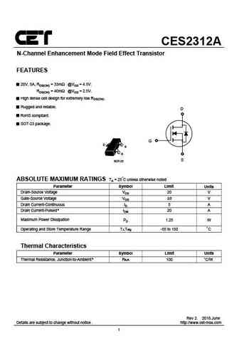
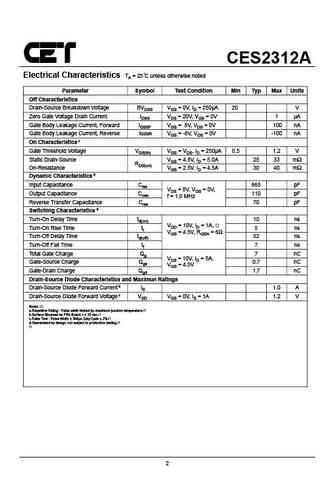
CES2312A N-Channel Enhancement Mode Field Effect Transistor FEATURES 20V, 5A, RDS(ON) = 33m @VGS = 4.5V. RDS(ON) = 40m @VGS = 2.5V. High dense cell design for extremely low RDS(ON). Rugged and reliable. D RoHS compliant. SOT-23 package. G D S G S SOT-23 ABSOLUTE MAXIMUM RATINGS TA = 25 C unless otherwise noted Parameter Symbol Limit Units Drain-Source Voltage VDS 20 V Gate-Source Voltage VGS 8 V Drain Current-Continuous ID 5 A Drain Current-Pulsed a IDM 20 A Maximum Power Dissipation PD 1.25 W Operating and Store Temperature Range TJ,Tstg -55 to 150 C Thermal Characteristics Parameter Symbol Limit Units Thermal Resistance, Junction-to-Ambient b R JA 100 C/W Rev 2. 2018.June Details are subject to change without notice . http //www.cet-mos.com 1 CES2312A Electrical Characteristics TA = 25 C unless otherwise noted Parameter Symbol Test Condi... See More ⇒
Keywords - ALL TRANSISTORS SPECS
ces2312a.pdf Design, MOSFET, Power
ces2312a.pdf RoHS Compliant, Service, Triacs, Semiconductor
ces2312a.pdf Database, Innovation, IC, Electricity
BJT Parameters and How They Relate
🌐 : EN ES РУ

LIST
Last Update
BJT: ZDT6705 | GA1L4Z | GA1A4M | SBT42 | 2SA200-Y | 2SA200-O
Popular searches
irfz44n | irf3205 | irfz44n datasheet | 2n4401 | bc547 transistor | bd139 | 2n4401 datasheet