View cezc2p07 detailed specification:
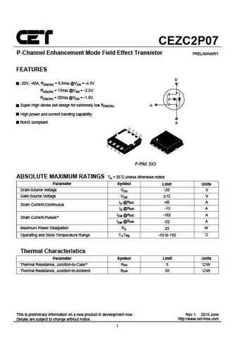
CEZC2P07 P-Channel Enhancement Mode Field Effect Transistor PRELIMINARY FEATURES D -20V, -40A, RDS(ON) = 9.5mW @VGS = -4.5V. RDS(ON) = 13mW @VGS = -2.5V. RDS(ON) = 20mW @VGS = -1.8V. G Super High dense cell design for extremely low RDS(ON). High power and current handing capability. RoHS compliant. S P-PAK 3X3 ABSOLUTE MAXIMUM RATINGS TA = 25 C unless otherwise noted Parameter Symbol Limit Units Drain-Source Voltage VDS -20 V Gate-Source Voltage VGS 12 V ID @RqJC -40 A Drain Current-Continuous ID @RqJA -13 A IDM @RqJC -160 A Drain Current-Pulsed a IDM @RqJA -52 A Maximum Power Dissipation PD W 25 Operating and Store Temperature Range TJ,Tstg -55 to 150 C Thermal Characteristics Parameter Symbol Limit Units Thermal Resistance, Junction-to-Case b RqJc 5 C/W Thermal Resistance, Junction-to-Ambient RqJA 50 C/W This is preliminary information on a new p... See More ⇒
Keywords - ALL TRANSISTORS SPECS
cezc2p07.pdf Design, MOSFET, Power
cezc2p07.pdf RoHS Compliant, Service, Triacs, Semiconductor
cezc2p07.pdf Database, Innovation, IC, Electricity
BJT Parameters and How They Relate
🌐 : EN ES РУ

LIST
Last Update
BJT: ZDT6705 | GA1L4Z | GA1A4M | SBT42 | 2SA200-Y | 2SA200-O
Popular searches
irfz44n | irf3205 | irfz44n datasheet | 2n4401 | bc547 transistor | bd139 | 2n4401 datasheet