View cb3139ktb detailed specification:
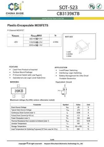
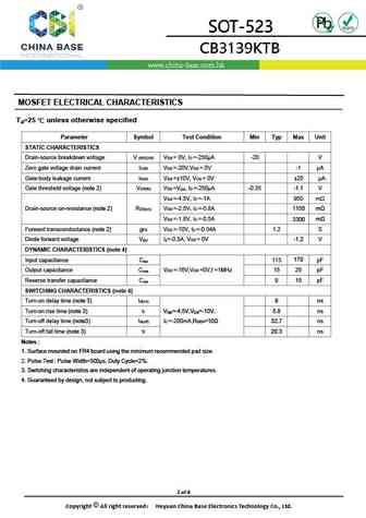
Plastic-Encapsulate MOSFETS P-Channel MOSFET I V(BR)DSS RDS(on)MAX D SOT-523 m @-4.5V 950 -20V -0.66A m 1150 @-2.5V 3300m @-1.8V 1. GATE 2. SOURCE 3. DRAIN FEATURE APPLICATION Lead Free Product is Acquired Load/Power Switching Surface Mount Package Interfacing, Logic Switching P-Channel Switch with Low R (on) DS Battery Management for Ultra Small Operated at Low Logic Level Gate Drive Portable Electronics MARKING Equivalent Circuit D G 39KB S Maximum ratings (T =25 unless otherwise noted) a Parameter Symbol Value Unit Drain-Source Voltage VDS -20 V Typical Gate-Source Voltage VGS 12 V Continuous Drain Current (note 1) I -0.66 A D Pulsed Drain Current (t =10 s) IDM -1.2 A p Power Dissipation (note 1) P 150 mW D Thermal Resistance from Junction to Ambient (note 1) R JA 833 /W Junction Temperature T 150 ... See More ⇒
Keywords - ALL TRANSISTORS SPECS
cb3139ktb.pdf Design, MOSFET, Power
cb3139ktb.pdf RoHS Compliant, Service, Triacs, Semiconductor
cb3139ktb.pdf Database, Innovation, IC, Electricity
BJT Parameters and How They Relate
🌐 : EN ES РУ

LIST
Last Update
BJT: ZDT6705 | GA1L4Z | GA1A4M | SBT42 | 2SA200-Y | 2SA200-O
Popular searches
irfz44n | irf3205 | irfz44n datasheet | 2n4401 | bc547 transistor | bd139 | 2n4401 datasheet