View tw1529sj detailed specification:
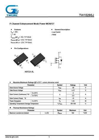
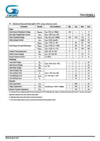
TW1529SJ P-Channel Enhancement Mode Power MOSFET Features General Description VDS = -30V, Load Switch ID = -4A PWM RDS(ON) @VGS= -10V, TYP 46m R DS(ON) @VGS= -4.5V, TYP 50m R DS(ON) @VGS= -2.5V, TYP 63m Pin Configurations SOT23-3L Absolute Maximum Ratings @T =25 unless otherwise noted A Parameter Symbol Ratings Unit Drain-Source Voltage VDSS -30 V Gate-Source Voltage VGSS 12 V TA=25 C -4 Drain Current (Continuous) *AC ID A TA=70 -3.2 C Drain Current (Pulse) *B IDM -15 A Power Dissipation TA=25 C PD 1.25 W Operating Temperature/ Storage Temperature TJ/TSTG -55 150 Thermal Resistance Ratings Parameter Symbol Maximum Unit Maximum Junction-to-Ambient t 5S R 100 C/W thJA www.tw-gmc.com 1 TW1529SJ Electrical Characteristics @T =25 unless otherwise noted A Parameter Sy... See More ⇒
Keywords - ALL TRANSISTORS SPECS
tw1529sj.pdf Design, MOSFET, Power
tw1529sj.pdf RoHS Compliant, Service, Triacs, Semiconductor
tw1529sj.pdf Database, Innovation, IC, Electricity
🌐 : EN ES РУ

LIST
Last Update
BJT: GA1A4M | SBT42 | 2SA200-Y
Popular searches
irfz44n | irf3205 | irfz44n datasheet | 2n4401 | bc547 transistor | bd139 | 2n4401 datasheet