View j309 j310 mmbfj309 mmbfj310 detailed specification:
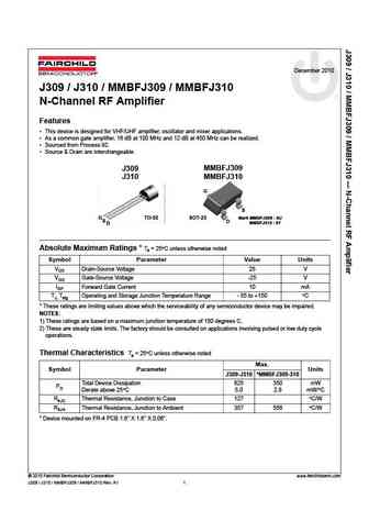
December 2010 J309 / J310 / MMBFJ309 / MMBFJ310 N-Channel RF Amplifier Features This device is designed for VHF/UHF amplifier, oscillator and mixer applications. As a common gate amplifier, 16 dB at 100 MHz and 12 dB at 450 MHz can be realized. Sourced from Process 92. Source & Drain are interchangeable. J309 MMBFJ309 J310 MMBFJ310 G S SOT-23 G TO-92 Mark MMBFJ309 6U S D MMBFJ310 6T D Absolute Maximum Ratings * Ta = 25 C unless otherwise noted Symbol Parameter Value Units VDS Drain-Source Voltage 25 V VGS Gate-Source Voltage -25 V IGF Forward Gate Current 10 mA TJ, Tstg Operating and Storage Junction Temperature Range - 55 to +150 C * These ratings are limiting values above which the serviceability of any semiconductor device may be impaired. NOTES 1) These ratings are based on a maximum junction temperature of 150 degrees C. 2) Th... See More ⇒
Keywords - ALL TRANSISTORS SPECS
j309 j310 mmbfj309 mmbfj310.pdf Design, MOSFET, Power
j309 j310 mmbfj309 mmbfj310.pdf RoHS Compliant, Service, Triacs, Semiconductor
j309 j310 mmbfj309 mmbfj310.pdf Database, Innovation, IC, Electricity
