View j309 j310 mmbfj309 mmbfj310 datasheet:
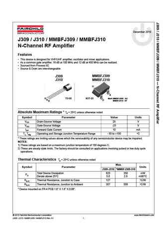
December 2010J309 / J310 / MMBFJ309 / MMBFJ310N-Channel RF AmplifierFeatures This device is designed for VHF/UHF amplifier, oscillator and mixer applications. As a common gate amplifier, 16 dB at 100 MHz and 12 dB at 450 MHz can be realized. Sourced from Process 92. Source & Drain are interchangeable.J309 MMBFJ309J310 MMBFJ310GSSOT-23G TO-92 Mark MMBFJ309 : 6USD MMBFJ310 : 6TDAbsolute Maximum Ratings * Ta = 25C unless otherwise noted Symbol Parameter Value UnitsVDS Drain-Source Voltage 25 VVGS Gate-Source Voltage -25 VIGF Forward Gate Current 10 mATJ, Tstg Operating and Storage Junction Temperature Range - 55 to +150 C* These ratings are limiting values above which the serviceability of any semiconductor device may be impaired.NOTES:1) These ratings are based on a maximum junction temperature of 150 degrees C.2) Th
Keywords - ALL TRANSISTORS DATASHEET
j309 j310 mmbfj309 mmbfj310.pdf Design, MOSFET, Power
j309 j310 mmbfj309 mmbfj310.pdf RoHS Compliant, Service, Triacs, Semiconductor
j309 j310 mmbfj309 mmbfj310.pdf Database, Innovation, IC, Electricity


LIST
Last Update
BJT: GA1A4M | SBT42 | 2SA200-Y | 2SA200-O | 2SD882-Q | 2SD882-P | 2SD882-E | 2SC945-L | 2SC945-H | 2SC4226-R23 | 2SC3357-F | 2SC3357-E | 2SC3356-R26 | 2SC3356-R24 | 2SC3356-R23 | 2SB772-Q | 2SB772-P | 2SB772-E | 2SA1015-L | 2SA1015-H | HSS8550
Popular searches
irfz44n | irf3205 | irfz44n datasheet | 2n4401 | bc547 transistor | bd139 | 2n4401 datasheet