View pf5102 detailed specification:
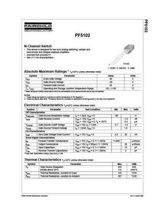
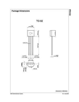
PF5102 N-Channel Switch This device is designed for low level analog switching, sample and hold circuits and chopper stabized amplifiers. Sourced from process 51. See J111 for characteristics. TO-92 1 1. Drain 2. Source 3. Gate Absolute Maximum Ratings * TA=25 C unless otherwise noted Symbol Parameter Value Units VDG Drain-Gate Voltage 40 V VGS Gate-Source Voltage -40 V IGF Forward Gate Current 50 A TJ, TSTG Operating and Storage Junction Temperature Range -55 +150 C * These ratings are limiting values above which the serviceability of any semiconductor device may be impaired. NOTES 1. These ratings are based on a maximum junction temperature of 150 degrees C. 2. These are steady state limits. The factory should be consulted on applications involving pulsed or low duty cycle operations. Electrical Characteristics TA=25 C unless otherwise noted S... See More ⇒
Keywords - ALL TRANSISTORS SPECS
pf5102.pdf Design, MOSFET, Power
pf5102.pdf RoHS Compliant, Service, Triacs, Semiconductor
pf5102.pdf Database, Innovation, IC, Electricity
