View 2n2913 2n2915 2n2917 detailed specification:
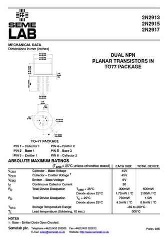
2N2913 2N2915 2N2917 MECHANICAL DATA Dimensions in mm (inches) 8.51 (0.335) 9.40 (0.370) DUAL NPN 7.75 (0.305) 8.51 (0.335) PLANAR TRANSISTORS IN TO77 PACKAGE 1.02 (0.040) Max. 0.41 (0.016) 0.53 (0.021) 5.08 (0.200) 2.54 (0.100) 4 2.54 5 (0.100) 0.74 (0.029) 3 6 1.14 (0.045) 2 1 45 0.71 (0.028) 0.86 (0.034) TO 77 PACKAGE PIN 1 Collector 1 PIN 4 Emitter 2 PIN 2 Base 1 PIN 5 Base 2 PIN 3 Emitter 1 PIN 6 Collector 2 ABSOLUTE MAXIMUM RATINGS (Tamb = 25 C unless otherwise stated) EACH SIDE TOTAL DEVICE VCBO Collector Base Voltage 45V VCEO Collector Emitter Voltage 1 45V VEBO Emitter Base Voltage 6V IC Continuous Collector Current 30 PD Total Device Dissipation TAMB = 25 C 300mW 500mW Derate above 25 C 1.72mW / C 2.86W / C PD Total Device Dissipation TC = 25 C 750mW 1.5W Derate above 25 C 4.3mW /... See More ⇒
Keywords - ALL TRANSISTORS SPECS
2n2913 2n2915 2n2917.pdf Design, MOSFET, Power
2n2913 2n2915 2n2917.pdf RoHS Compliant, Service, Triacs, Semiconductor
2n2913 2n2915 2n2917.pdf Database, Innovation, IC, Electricity
BJT Parameters and How They Relate
🌐 : EN ES РУ

LIST
Last Update
BJT: ZDT6705 | GA1L4Z | GA1A4M | SBT42 | 2SA200-Y | 2SA200-O
Popular searches
irfz44n | irf3205 | irfz44n datasheet | 2n4401 | bc547 transistor | bd139 | 2n4401 datasheet