View ssm3j111tu detailed specification:
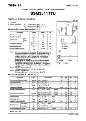
SSM3J111TU TOSHIBA Field Effect Transistor Silicon P-Channel MOS Type SSM3J111TU High Speed Switching Applications Unit mm 2.5V drive 2.1 0.1 Low on-resistance Ron = 480m (max) (@VGS = -4 V) 1.7 0.1 Ron = 680m (max) (@VGS = -2.5 V) Absolute Maximum Ratings (Ta = 25 C) 1 3 2 Characteristic Symbol Rating Unit Drain-Source voltage VDS -20 V Gate-Source voltage VGSS 12 V DC ID -1 Drain current A Pulse IDP -2 PD (Note 1) 800 Drain power dissipation mW PD (Note 2) 500 1 Gate Channel temperature Tch 150 C 2 Source 3 Drain Storage temperature range Tstg -55 150 C UFM Note Using continuously under heavy loads (e.g. the application of high temperature/current/voltage and the significant change in temperature, etc.) may cause this product to decrease in the JEDEC reliability significantly even if the operatin... See More ⇒
Keywords - ALL TRANSISTORS SPECS
ssm3j111tu.pdf Design, MOSFET, Power
ssm3j111tu.pdf RoHS Compliant, Service, Triacs, Semiconductor
ssm3j111tu.pdf Database, Innovation, IC, Electricity
🌐 : EN ES РУ

LIST
Last Update
BJT: GA1A4M | SBT42 | 2SA200-Y
Popular searches
irfz44n | irf3205 | irfz44n datasheet | 2n4401 | bc547 transistor | bd139 | 2n4401 datasheet