View 2n7002dw datasheet:
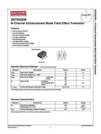
October 20072N7002DWN-Channel Enhancement Mode Field Effect TransistorFeatures Dual N-Channel MOSFET Low On-Resistance Low Gate Threshold Voltage Low Input Capacitance Fast Switching Speed Low Input/Output Leakage Ultra-Small Surface Mount Package Lead Free/RoHS CompliantSC70-6 (SOT363)11Marking : 2NAbsolute Maximum Ratings * Ta = 25C unless otherwise notedSymbol Parameter Value UnitsVDSS Drain-Source Voltage 60 VVDGR Drain-Gate Voltage RGS 1.0M 60 VVGSS Gate-Source Voltage Continuous 20VPulsed 40ID Drain Current Continuous 115Continuous @ 100C 73 mAPulsed 800TJ , TSTG Junction and Storage Temperature Range -55 to +150 C* These ratings are limiting values above which the serviceability of any semiconductor device may by impaired.Thermal CharacteristicsSymbol Parameter Value UnitsPD Tot
Keywords - ALL TRANSISTORS DATASHEET
2n7002dw.pdf Design, MOSFET, Power
2n7002dw.pdf RoHS Compliant, Service, Triacs, Semiconductor
2n7002dw.pdf Database, Innovation, IC, Electricity


LIST
Last Update
BJT: GA1A4M | SBT42 | 2SA200-Y | 2SA200-O | 2SD882-Q | 2SD882-P | 2SD882-E | 2SC945-L | 2SC945-H | 2SC4226-R23 | 2SC3357-F | 2SC3357-E | 2SC3356-R26 | 2SC3356-R24 | 2SC3356-R23 | 2SB772-Q | 2SB772-P | 2SB772-E | 2SA1015-L | 2SA1015-H | HSS8550
Popular searches
irfz44n | irf3205 | irfz44n datasheet | 2n4401 | bc547 transistor | bd139 | 2n4401 datasheet